

mikroBUS module dimensions
 Peter Jakacki
Posts: 10,193
Peter Jakacki
Posts: 10,193
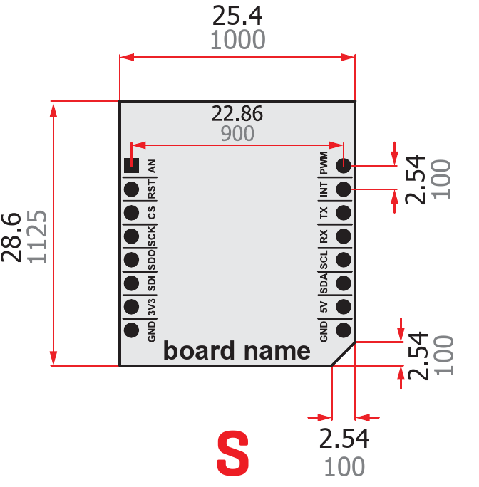
I've read the spec and created footprints for the socket and modules but I'm a little confused, all due to one single dimension that is missing. The socket is 1125mils long and seems to extend back 150mils from the back of the pin header. That is clear in the drawings but the plug-in module is the same length but seems to extend 100mils back yet there is no dimensions to indicate this, only the chamfer indicates this.
So according to what I can interpret, the module outline would extend up and out of the open end of the socket outline by 50mil? Sure, this might seem a minor point but I know too well the importance of accurate footprints. Just wanted to confirm all this before I hit the make button.
I haven't had another look at this since late last night, so maybe I just need a cup of coffee.
764 x 753 - 65K

672 x 684 - 45K
Comments
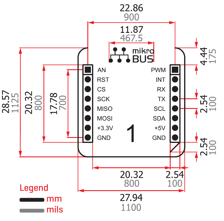
The sideways pitch of sockets is 1150 mil, they add an extra 50 mil in between what you have shown above
The socket outline is 1.1" but the module is 1" allowing for a gap.
btw - I did make one other assumption, that the 900 pitch rows are centered on the 1000 outline. While that is a safe assumption, you shouldn't have to assume.
I can look and take a guess but the result is the module sticks out 50mil from the top of the matching socket outline which seems strange. Get it?
Btw, those outlines are the spec itself.
That's right, it's a sloppy drawing and if it were a machine/pcb file it would fail. But the consequence of the guessing is that the top of the plug-in module protrudes 50mil above the top of the socket outline. You would think that the socket outline would contain the module inline completely. If this is the only source of information about the dimensions then no wonder there is dimensional disparity among manufacturers.
EDIT: Here are the pcb footprint outlines I constructed from the drawings for socket and module. The socket is the broad tan outlines and the module footprint has been dropped over it with the thin brown outline. Notice the top of it protrudes the socket outline on the right side, which is the top. Of course I can live with it, that's not my problem. But if I had an smd component that had ambiguous dimensions on it I would try to use another brand that was clearer or at least have a sample I could measure, which isn't easy. Electrical "dimensions" or voltages are easy, they are always referenced to the common or ground. Mechanical dimensions can have multiple references (often missing) especially when it comes to the contacts part vs the body part.
Mechanical drawings I’ve seen from other industries usually have a singular reference point from where all dimensions emanate from.
Connector dimensions often seem to have the pins all relative to each other, and the case dimensions again relative to each other, but what’s often missing is the relationship (measurement) between the two sections. And just to add to the confusion, measurements are often relative to another measurement, rather than back to a reference point. Plus, often there are missing critical measurements missing too, necessitating bringing out the calipers to try and measure them.
- Arduino has that 0.160" offset between top headers
- Mikrobus seem to have this 0.050" unaccounted for
- pmod have pin 1 as the gpio pin, rather than GND
So the question is, what will be the P2D2 quirk that makes it a runaway success ?
I have one of the v8 development boards, they don't bother with the shorter outline, the height of the socket on the silk screen is around 2.4"
That's easy enough for simpler boards but still not accurate. Even if the printer was a real 1200dpi and I printed on polyester, you couldn't check the mating to the pads under some parts. I might use this method just to check the placement and "feel" of the main connectors, but that's about it as it is a poor substitution for accurate footprints and outlines.
Have you never created footprints? Have you tried to follow the drawings? Have you tried to work out whether they are showing you the bottom or top view because it is such a mess? What is the recommended pcb pad size. This is sheer frustration for many components and having to check and create footprints for new components can take quite a while.
The point of this whole thread was not about me being worried or that I couldn't get it right, as I have done many hundreds of tight pcb designs, it is about the discrepancies in mechanical drawings of components. In this case a European company which normally care about small details and because they are setting the standard, they should know and understand the details. Who there is checking what is published?
Last month I sent a request for mechanical dimensions late Friday night, they responded within an hour that they'd have the info to me Monday, which they did
I haven't seen any of your tight pcb designs that you have done, or any other ones either so I don't know where you are coming from with those generalities. They used to refer to pcb designs as "artwork" and if done well they could be a work of art, but to get there sure was 'art work
None of this is slowing me up at all, just sharing my thoughts.