

Cluso's SAP Computer
 Cluso99
Posts: 18,069
Cluso99
Posts: 18,069
For some time now I have wanted to build a "Simple As Possible" computer along the lines of the SAP-1.
It's been done with all transistors, just gates, just EEPROMs, and of course an FPGA.
I have thought about building it with a set of common configurable gates such as the 74LVC99, perhaps just latches, etc.
Over recent weeks I thought about using cheap micros to replace the blocks of configurable logic, meaning a small number (4-7) of the same micro. I have looked at AVR ATTiny's, 8051's, and ARM's. I have also considered using just small/cheap iCE40 FPGA's.
I would make each block on a common board and stack them together.
Thinking about the display to see what is happening, a set of LEDs would be required for
To get the ball rolling, I decided that a small/cheap LCD would be good. I have used these in Prop projects before.
So, for now, I am going to build this computer with a Propeller chip using my P8XBlade2.
I will use a core/cog for each of the following logic blocks...
Each of the logic blocks will comunicate using a 12-bit Bus using Propeller external I/O...
The LCD display (Bus Monitoring) will also derive it's display states from the 12-bit Bus
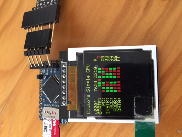
Here is a picture of the LCD display. The states 0-7 are being simulated, and the other registers are currently just fixed.
Sorry, the forum software has decided to rotate the image It's fine on my iPhone and PC.
It's been done with all transistors, just gates, just EEPROMs, and of course an FPGA.
I have thought about building it with a set of common configurable gates such as the 74LVC99, perhaps just latches, etc.
Over recent weeks I thought about using cheap micros to replace the blocks of configurable logic, meaning a small number (4-7) of the same micro. I have looked at AVR ATTiny's, 8051's, and ARM's. I have also considered using just small/cheap iCE40 FPGA's.
I would make each block on a common board and stack them together.
Thinking about the display to see what is happening, a set of LEDs would be required for
* STATE
* PC (program counter)
* IR (instruction register)
* ACC (Accumulator A which also stores the ALU result)
* ADDR (Address - memory and input/output)
* DATA (Data - to/from memory/io)
* PC (program counter)
* IR (instruction register)
* ACC (Accumulator A which also stores the ALU result)
* ADDR (Address - memory and input/output)
* DATA (Data - to/from memory/io)
To get the ball rolling, I decided that a small/cheap LCD would be good. I have used these in Prop projects before.
So, for now, I am going to build this computer with a Propeller chip using my P8XBlade2.
I will use a core/cog for each of the following logic blocks...
* PC
* IR (and State/Reset/Clock and control)
* ACC & ALU
* Memory
* Input/Output
plus 2 cores/cogs for...
* IR (and State/Reset/Clock and control)
* ACC & ALU
* Memory
* Input/Output
* Bus monitoring for LCD display (spin for now)
* LCD Driver (pasm)
* LCD Driver (pasm)
Each of the logic blocks will comunicate using a 12-bit Bus using Propeller external I/O...
* P00..P07: Address/Data bus (8 bits)
* P08..P10: States 0-5 (although I can expand to 8 states)
* P11: /Reset
* P08..P10: States 0-5 (although I can expand to 8 states)
* P11: /Reset
The LCD display (Bus Monitoring) will also derive it's display states from the 12-bit Bus
Here is a picture of the LCD display. The states 0-7 are being simulated, and the other registers are currently just fixed.
Sorry, the forum software has decided to rotate the image
640 x 480 - 105K
Comments
However I think using micro-controllers to do it is cheating.
At that point you may as well just write some Verilog and put it all into an FPGA.
Getting my own design SAP computer written in Verilog for an FPGA is on my TODO list.
If I could build it using TTL I would be over the moon.
Interesting..
The 8051 should win at pure logic replacement, as it has native boolean opcodes.
However, once you get 4-7 MCUs (and that's likely to creep up) the management of all those hex files becomes an issue...and speed is never going to be much. A development dead end really.
I favour the iCE40UP5K–SG48, as that has a compact package and 128kB of SRAM.
Think of this as 'smart memory'...
Add a small MCU to that for ADC features...
In looking at SAP designs, I've decided the memory is pivotal: The ALU/CORE is simple, and a dime a dozen, but ones optimised to execute from low cost, small size memory are rarer.
Highest bandwidth comes from QuadSPI and HyperFLASH, with DDR/DTR options (both clock edges used).
Digikey shows
FT25H16T-RB FLASH 16MBIT 120MHZ 8TSSOP $0.14553 @ 1000
and higher performance BUS speed....
IS25LP080D-JNLE ISSI, 8MBIT 133MHZ 8SOIC $0.77000 @ 1000 8Mb (1M x 8 ) 133MHz SPI-MIO, QPI, DTR 2.3 V ~ 3.6 V -40°C ~ 105°C (TA) 8-SOIC (0.154", 3.90mm Width) 8-SOP
The latter has dual edge transfers, so has the lowest latency. The former is very cheap..
Currently I intend on extending to 16 possible instructions (ADD, ADDC, SUB, SUBC, AND, OR, XOR, NOT, LDA, STA, OUT, IN, JMP, JZ, JM, JC.
Memory will be 256 Bytes and at this stage I/O will be 1x 8bit output and 1x8bit input plus a serial input and output. The memory and address latch and the serial I/O will be done by 1 cog. The 256 Bytes of RAM will be internal to the cog - there will not be an external ram chip.
Each cog (or micro or tiny fpga) is just performing a predefined function for a set of logic chips in software. I am not emulating a SAP computer.
Each cog will only communicate via the external 12 bit bus (I/O pins).
Once I have completed this to my satisfaction, I will probably build board(s), one each to replace a cog, one at a time, until I end up with the prop just monitoring the bus and displaying the states etc on the LCD.
I have the 6 required states worked out. Here is an example for LDA <address>
PC++
RAM[PC] data onto bus and latched into Instruction Register
PC onto bus for fetching operand
PC++
RAM[PC] data onto bus and for LDA latch into ACC
Speed is not important. It is likely to be deliberately slowed so that the states can be followed. Perhaps I will even allow single stepping of states.
While I have never used an 8051 I am fully aware of its base instruction set. During the pre-release I was deciding whether to use an 8751 or a 68705. I chose 68705 which also has bit instructions, which is what I needed for my projects. Started shipping product prior to official Motorola release. There was a pair on one of my products and not much else - they cost $175 ea back then. Later shipped about 250,000 pcs in 3 years in my modem designs - fortunately their price was down to $20 at the start and $8 at the end.
Don't agree with your obsession with QSPI.
Except I imagined building an ALU from TTL, using a few old 2K RAM chips I have gathering dust for memory. That and the registers, in TTL, all lashed together with whatever MUXs. Then the control sequencer would have been a Propeller.
Once the control sequence microcode was perfected in PASM it could then be reimplemented with an EPROM based state machine.
Interesting, but if this is all inside a Prop, how does anyone 'see' the slowed down states ?
There is no obsession, if you have any alternatives for lowest cost memory, I'm all ears
The market has chosen SPI, I simply follow those enormous volumes, and select what is available.
If you make that bus externally visible, you could probe that, to show operation.
There were smarter byte-wide memory bus designs, that never hit widespread commercial critical mass.
One design added ALE pin, so the memory contained the latch. (I have some internal latch EPROMs here.)
Another design added an address increment on read (similar to what all Serial memories do)
I think some game cartridge ROMs used the multiple ALE design.
This is how today's byte-wide memory could have looked, had lowest-common-denominator not won... Mode Select can define who the transaction is for, ie include Chip-select by ID.
Memory address is a loadable counter, with increment ability. (+adder ability, if Aa has signed option)
Using this BUS design can shave a couple of states from the BUS
The 12bit bus is external to the prop. It's just that each cog is using it to perform the logic block. So, in fact, the monitor/LCD cogs are doing precisely what you suggest, monitoring the bus and displaying this on the LCD in real time. That's why the clock and states need to be slow.
My intended audience is for those that do not understand how a computer works. That's also why it doesn't need a lot of memory, and also tricks to make it faster.
BTW a number of micros (back when they were external data/address busses) used ALE. Essentially that is what my external state bus does.
You will see that I use a separate state to perform PC++. This could actually be done in parallel with either the previous or next state. I have chosen to break it out to show what is really happening.
I may even break the ALU state out into an extra state to show how the ALU takes the ACC and DATA bus as two inputs, plus a set of function bits latched and decoded from the Instruction read state, and performs the calculation, putting the result via a latch. The following state would take this latch data and place it back onto the DATA bus where the ACC would now read it in as the new result.
We have quite similar thoughts. I totally understand how the ALU logic works. The Singer/ICL mini that I cut my teeth on was all straight 74xx gates (ie 7400 etc, not 74LSxx or later). That was pre Intel 8008. I used to repair the logic boards and teach field engineers how the computer worked so they could board swap to get the customer back running quickly. If they couldn't I had to fly in and fix it. I also taught programming this mini. It's actually amazingly similar to the prop... memory to memory instructions (16 total), 20 processors with their own memory eg cog + cog memory, an common memory shared between the cores (eg hub memory). The multiple processors were actually one CPU hardware time sliced. BTW it was all decimal, so multiply A by B was decimal 10 digits each, with a 20 digit result into B. You had to be careful to allow the additiona space in B for the longer result. Memory (core) was also addressed decimally.
Emulating a SAP would be trivial:
' {$STAMP BS2}
' {$PBASIC 2.5}

LDA       CON   0
ADD       CON   1
SUB       CON   2
OUT       CON   14
HLT       CON   15

Memory    VAR   Byte(16)
AReg      VAR   Byte
IReg      VAR   Byte
OpCode    VAR   IReg.HIGHNIB
MemAd     VAR   IReg.LOWNIB
PReg      VAR   Nib

Load:
  Memory(0) = (LDA * 16) + $A     'lda contents 10
  Memory(1) = (ADD * 16) + $B     'add contents 11
  memory(2) = (SUB * 16) + $C     'sub contents 12
  memory(3) = (OUT * 16)          'display results
  memory(4) = (HLT * 16)
  memory(10) = 25
  memory(11) = 35
  Memory(12) = 55

DO
  IReg = Memory(PReg)
  DEBUG "PReg = ", BIN4 PReg, "   IReg = ", BIN4 OpCode, " ", BIN4 MemAd
  SELECT OpCode
    CASE LDA
      AReg = Memory(MemAd)
      DEBUG  "  AReg: ", BIN8 AReg, CR

    CASE ADD
      AReg = AReg + Memory(MemAd)
      DEBUG  "  AReg: ", BIN8 AReg, CR

    CASE SUB
      AReg = AReg - Memory(MemAd)
      DEBUG  "  AReg: ", BIN8 AReg, CR

    CASE OUT
      DEBUG "  Display Register: ", BIN8 AReg, CR

    CASE HLT
      DEBUG "  Program Terminated"
      END

    CASE ELSE
      DEBUG "  Invalid Instruction"
      END

    ENDSELECT
  Preg = Preg + 1
 LOOP
END
But it might be instructive.
An open collector ACK line may be useful to keep everything from losing sync ?
Sounds like the LCD sniffer would have variable impact on BUS.
Many still do have ALE, but the details where my expanded BUS above differs from 'older ALE', are
* ALE acts on both edges
* ALE can optionally repeat, to send address > 8 bits, still on same pin count bus.
* ALE is not mandated at one-per RW, the increment on RW allows straight-line-bursts, with no ALE
Just found the right 74xx chips for you!
Also found where potatohead has been hiding
74Gxx GHz chips
Cannot recall if any of the old micros took advantage of skipping the ALE if there was no change in the upper address bits. I would quite expect that may have happened on some of the old minis though. Some really pushed the envelope.
And that was most likely the trigger for RAS & CAS in DRAMs.
You may recall, the Z80 put out a hidden refresh making it well suited to DRAMs whereas most other micros back then were using SRAMs of specially built DRAM boards.
Who would have thought it.
We will soon have Intel on the run with those
Found a framed poster of the 386 or 486 die when my mum moved. I had a poster of both from Intel, and was storing them there.
It would be nice to put that IP into the P2
Waiting to see who gobbles them up???
The data sheets are oldish (~2010), and the > 1G specs are at very low CL (2pF), so I'm not sure it is so much a technical leap ...
Most other Logic families spec at 15pF and 50pF, and will of course be faster with 2pF loads.
eg The Potato 7474 specs 600MHz, whilst I see a NXP 74LVC1G79 can be had sub 10c, and gives 500MHz typ toggle.
PC: uses 2x 74xx161 & 1x 74xx373
ALU: uses 5x 74xx373, 2x 74xx86 (XOR) or 1x 74xx240 & 1x 74xx241, some gates or 74xx138/139 for decoding and perhaps another 74xx373, plus the actual ALU which can be built from gates
MEM: uses 74xx373 and RAM such as IS61LV256AL (only 256x8bit used)
I/O (2x 8bit input and 2x 8bit output): uses 5x 74xx373 & 1x 74xx138 (or gates)
Note this version has a wider control bus rather than a state bus.
The 74xx540/541 are preferred over the 74xx240/241 due to preferred pinout.
Probably the ALU would be better built from gates because it's then possible to ensure the basic ADD/ADDC/SUB/SUBC/AND/OR/XOR are supported.
plus it allows you to quite literally remap the opcodes anytime you want...
Just needs a macro assembler, to generate the large memory map...
Those are fast! Love the name.
I've been buried in a little P1 work. It's handed off now. Did it's job, and some other much more complex beast is taking over.
Also tooling. Lots of geometry. Love geometry problems.
IMHO no point in building a decent computer unless it's fast, like 500+MHz clocking, and 32bit.
Found some SRAMs starting at 500MHz $50 GS8342DT38BGD-500I 1Mx36 at Mouser, or these 1GHz $276 CY7C4142KV13-106FCXC 4Mx36. But they are BGA165 and FCBGA361
Setting my sights a little lower and TQFP100 and I see...
$15 512Kx36 250MHz GS8160Z36DGT-250I
$32 1Mx36 250MHz GS8320Z36AGT-250I
$80 2Mx36 250MHz GS8640Z36GT-250I
$124 4Mx36 250MHz GS8128036GT-250I
or non-stocked 400MHz 1Mx36 $47, 4Mx36 $172
Of course this not the current intended audience of my SAP design.
While there I had a chest infection, and been visiting specialists since I returned
Anyway, dug this out again. I realised it would be better to do the sequencer a bit different, and save some pins. The Data/Address Bus is 8 bits, there is an internal 6 Tstate clock for each instruction, and an external 16 Qstate (4 bit) bus for decoded operations (not all used), together with a clock Qclock (1bit).
This means a 13 bit bus.
The "SEQUENCER" Cog is now done (untested) in Spin.
My LCD can be used to display the various states and data on the bus using two other cogs.
I need a Cog for each of the other blocks...
* PC: Program Counter. Four active Q states are:
-- PC = 0 (reset)
-- PC++ (increment PC)
-- Read PC (for fetching instructions)
-- Write PC (for Jumps)
* ALU: Arithmetic and Logic Unit. Also contains the ACC (A accumulator and the 1st ALU input), the B (temporary register for the 2nd ALU input), IR[7:4] (Instruction Register top 4 bits which contain the instruction opcode). Active Q states:
-- Write ACC (latches either A data, or the ALU result)
-- Read ACC
-- Write B register
* Memory: RAM/Register Memory. Also contains the MAR (Memory Address Register). Initially MAR will only be 4 bits, but later expansion to 8 bits. Active Q states:
-- Write MAR
-- Read Memory using MAR
-- Write Memory using MAR (later)
* Input and Output Registers (1 each of 8 bits). Active Q states:
-- Read Input (later)
-- Write Output
Initially I will code in Spin. Later maybe I will convert to PASM.
Then I may build each block externally. Maybe with gates, maybe with a tiny FPGA. We will see
Currently expecting the following instructions to be ultimately supported:
ADD
ADDC
SUB
SUBC
AND
OR
XOR
NOT
LDA
STA
IN
OUT
JMP
JNZ
JNC
-spare- maybe RLC or RRC?
Good to be able to slow down enough to watch the CPU operate. We could single step each state on the mini I used to work on.