

MCP3202 (ADC) is leaking current through channel pin when ADC is powered down. What to do?
 Mahonroy
Posts: 175
Mahonroy
Posts: 175
in Propeller 1
Hey guys,
I designed a battery powered circuit using the Parallax Propeller. I am using a timer chip connected to the "shutdown" pin of a voltage regulator to put majority of the circuit into sleep mode for extended periods of time. This portion works great and successfully cuts off the 3.3V rail that everything is powered from.
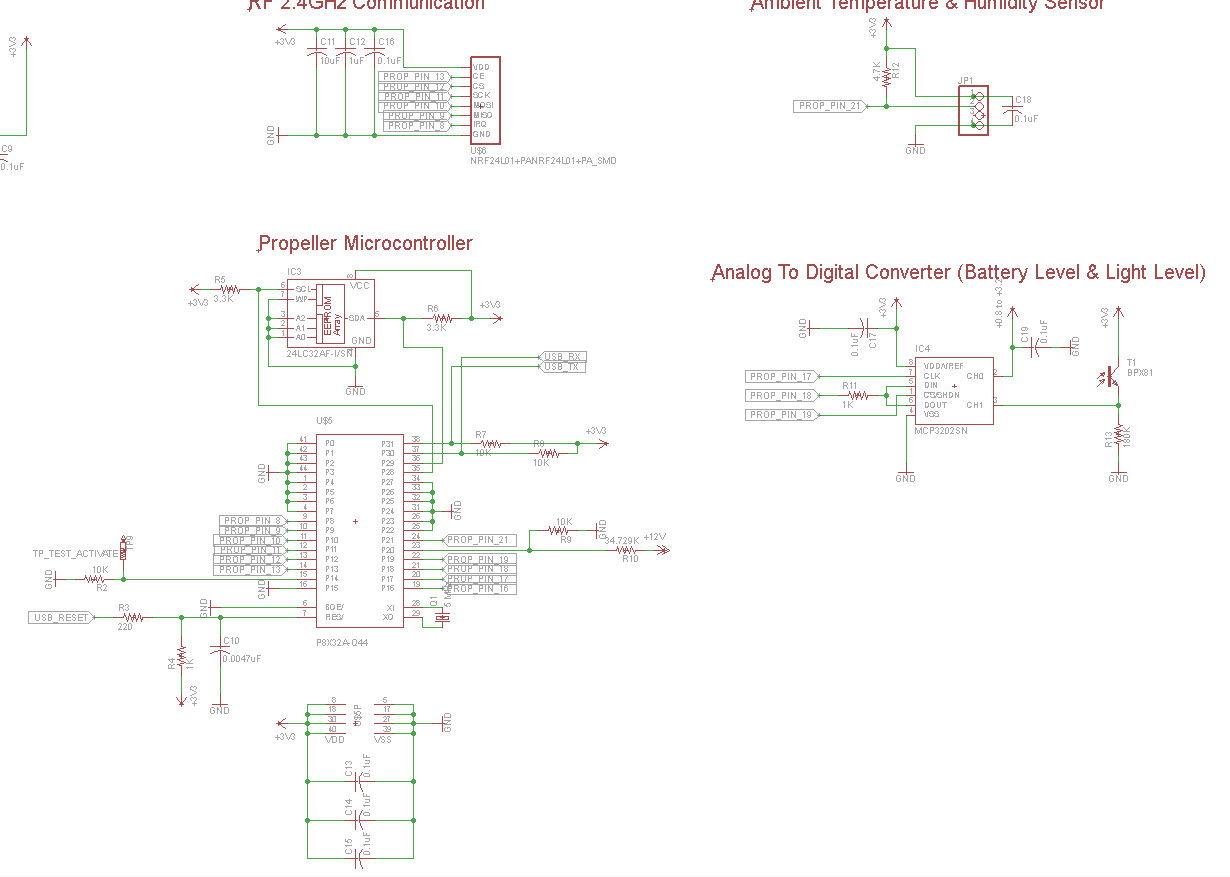
My problem is that I am using an MCP3202 (analog-to-digital converter) that has one of its channel input pins connected to the battery source. I am doing this so I can get a nice 0-100% battery remaining value.
When the 3.3V rail is shut down, voltage from the batteries goes through the MCP3202 channel and ends up bringing the 3.3v rail back up to like 2.5 volts and causes a 5mA current drain. Disconnecting the battery from the channel input solves the problem and there is no current leakage.
Is there an easy solution to this? I keep wondering if I can toss a diode in somewhere and be done with it, or if I need to get complicated with this and incorporate mosfets/transistors connected to GPIO of Propeller chip.
What do you guys think? Any help is greatly appreciated, thanks!
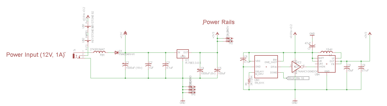
Below is my circuit schematic:
I designed a battery powered circuit using the Parallax Propeller. I am using a timer chip connected to the "shutdown" pin of a voltage regulator to put majority of the circuit into sleep mode for extended periods of time. This portion works great and successfully cuts off the 3.3V rail that everything is powered from.
My problem is that I am using an MCP3202 (analog-to-digital converter) that has one of its channel input pins connected to the battery source. I am doing this so I can get a nice 0-100% battery remaining value.
When the 3.3V rail is shut down, voltage from the batteries goes through the MCP3202 channel and ends up bringing the 3.3v rail back up to like 2.5 volts and causes a 5mA current drain. Disconnecting the battery from the channel input solves the problem and there is no current leakage.
Is there an easy solution to this? I keep wondering if I can toss a diode in somewhere and be done with it, or if I need to get complicated with this and incorporate mosfets/transistors connected to GPIO of Propeller chip.
What do you guys think? Any help is greatly appreciated, thanks!
Below is my circuit schematic:
1564 x 432 - 101K
1230 x 877 - 196K
Comments
A resistor as kwinn suggests might be effective since it will lower the current through the outlines protection diode leak mentioned above. The resistor should go between the battery terminal and the input channel of the MCP3202. "Clamping" Vdd and Ground with a lower value resistor (1K or so) might also be effective, but you need to watch out that you don't draw excessive current during normal operations. Perhaps "gating" the clamping resistor with a transistor could be a solution.
To minimize this kind of leakage further, you really need two mosfets that are back to back between the positive battery terminal and the input to the MCP3202, where their default state is OFF and they are powered or turned ON only when voltage is present at the Vdd of the MCP3202. An off the shelf solution might be able to utilize a mosfet level shifter for I2C communications to serve as the back to back mosfet.
Datasheet reference:
http://ww1.microchip.com/downloads/en/DeviceDoc/21034D.pdf
Back to Back mosfet reference:
http://electronics.stackexchange.com/questions/179706/how-come-2-mosfet-chips-are-needed-in-protection-circuits
Of course this same 8-pin micro could replace the MCP3202 and output all the sense data automatically over the single I/O serial link and it is quite possible to receive that serial data using nothing more than a few lines of Spin code.
This if course does not help if you have gone ahead and designed and built a pcb already.
One way to deal with the measurement is to use a voltage divider with high resistances to bring the supply voltage down into the range of the ADC. Say 1MΩ and 250k for a 5:1 ratio. There will be a small error in the measurement due to the high source impedance, but it will be consistent and you can compensate for it in the firmware. The error will be smaller if you add a 0.1µF capacitor across the 250kΩ, so long as you don't read that channel more often than once a second or so. That reduces your constant battery drain to a few microamps.
I liked the idea of trying a diode between the 3.3V and the MCP 3.3V pin (pointing towards the MCP) since I can rig this up on an existing PCB to test. Would this extra diode basically nullify the input channels protection diode thats inside the ADC?
Is there a way to calculate what the current draw might be if I put this 10K resistor between the battery and the MCP? I am ok with doing a software correction.
Would this "clamping resistor" need to be some ratio based off the other resistor that goes between the battery and the MCP channel input? E.g. 20K in input, and 2K clamping?
Not a bad idea either thanks! This would be outside the scope of my capabilities, I have never programmed a PIC or AVR, though I am just starting to research more so I can dive into it.
I'm thinking the schematic part has an incorrect graphic. How its working is without the 12V power connector plugged in, the batteries are connected to ground (through the DC connector). When you insert the DC connector, the batteries become disconnected, and the DC power is then grounded in its place.
U$1 and U$2 are the battery components, each part consists of 2x of those Keystone 92 brackets to hold a battery.
And yes you are correct, the "0.8 to 3.2 volts" is the voltage rail created by 2x AA batteries connected in serial. And yes that is the voltage source that is currently perminantly connected to the ADC chanel input.
U$4 is a boost converter. It takes the battery power and converts it to a steady 3.3V only when the timer allows it to power up. Most of the time the boost converter is sitting in shutdown mode.
1. Put resistor between battery and ADC channel input.
2. Put voltage divider between battery and ADC channel input (was suggested to use a 1M ohm, and 200K ohm for a 5:1 ratio, and possibly a 0.1uF capacitor - btw I already have a 0.1uF cap there).
3. Put a resistor between battery, and a pull-down resistor on the ADC power pin.
For #2, won't the voltage divider bring the 3.3V down to 0.55V? Why drop it so much? Why not do it in the other configuration for a 1.2:1 ratio and have 3.3V turn into 2.75V? Is the pull-down portion of the voltage divider necessary?
Right now this device is sitting around only 5-10 microamps when in its shutdown state, so it would be cool to keep it in the vicinity I suppose
Thanks again guys for the great advice!
I thought maybe the ADC needed to measure the 12V external power when that is applied, but not so. No need for a 5:1 divider. For simplicity, I'd just go with a 1MΩ resistor per idea #1 and apply a correction in firmware if needed. Another resistor from the ADC CH0 pin to ground could reduce any tendency for the voltage at the ADC pin to provide parasitic power.
What boost IC are you using? Some boost IC's when in shutdown pass the input voltage directly through to the output, so the circuit remains powered but at the lower supply voltage. That can be a feature or a failure depending on how you plan it.
There is perhaps another patch to do with powering the A/D from the battery. But if designed from scratch I would use a small micro as I mentioned and it is easy to learn to use these chips but you might and should give yourself sometime in-between projects to tool up and learn as you normally do not require these chips to do anything too complicated that a few dozen lines of simple assembler can't fix. I use many different chips and although I love Silabs stuff I find that the PICs are in friendlier packages and more readily available at very good prices. My latest project uses PIC12F1572 chips in tiny 8-pin MSOP (or DIP) packages with A/D, UART, PWM, etc for around 50 cents.
btw, the extra ratio of the resistive divider is not that important as the voltage can be easily adjusted in software but the purpose is to limit the current/voltage but still I find that without a cutoff that this is still a kludge.
edit: a single analog switch for reference (powered from battery supply)
These load switches consist of a small n-channel mosfet coupled to a large power handling p-channel mosfet.
But that would be overkill. Following on Beau's comment, all it would really take is a discrete fet with its gate connected to DRVn circuit of the '5111, to enable or disable the connection of the battery to the ADC. Yet discrete mosfets are the same price each as the analog switches that Peter recommended, yet again, the wiring is a kiss and you could buy a discrete in a TO92 package.
See page two of the datasheet .... "Voltages exceeding V+ or GND on any signal terminal are clamped by internal diodes."
Datasheet reference:
http://www.ti.com/lit/ds/symlink/ts12a4515.pdf
:
Not with the CMOS switches if they are powered directly from the battery as mentioned, they will only draw around 0.05uA.
If you cut the power leaving the battery terminals positive supply being the highest voltage potential then the rule on page two of the datasheet will be broken through the input terminal ... "Voltages exceeding V+ or GND on any signal terminal are clamped by internal diodes." .... when this happens the clamping diodes will conduct and you are back where you started with the MCP3202 only with the switching IC instead.
For a pure 3 terminal transistor circuit there is no substrate potential to worry about. Here is an example using a mosfet with source to the battery, gate to the output of the inverter in the OP's circuit, and the drain to the ADC ch0. Also this can be done using a p-jfet or a PNP bipolar. The 1M resistor is there to absorb leakage current. The PNP transistor as a switch isn't quite as accurate but should be adequate in this situation. The pmosfet and the PNP need a low level on the gate(base) in order to turn on. The depletion mode p-jfet on the other hand needs a high level on its gate to turn on, so it can connect directly to the output of the timer chip TPL5111.
An issue is still the 0.8V minimum, if you really have to have that. It is hard to find p-mosfets or jfets with threshold below 0.8V without special selection. The PNP bipolar may in fact perform better at low battery voltage due to the sharper ~0.6V threshold. Esoteric note: PNP transistors used as analog switches are sometimes operated in inverted mode, that is, with the emitter and collector reversed. The gain is much lower, but the saturation error Vec is also lower.
I agree about the 2V battery limit. Even at 1V per cell, the cells will be almost comatose. I'm still wondering about the OP's boost converter, what is the part number. As you've pointed out a number of times shutdown on boost topologies usually turns off the boost but still passes the battery voltage thru to the output.
I am using a true shutdown boost converter which completely disconnects the output ( MAX1795 ).
So let me know if this will work and that I am understanding everything?
I need to find an analog switch that has a low minimum power value, and this IC's power will be permanently connected to the 2x batteries.
The enable pin of the switch will be connected to the generated boosted 3.3V rail, and will have like a 10K pulldown to ground.
The line that currently goes to the ADC channel input would be spliced, and the "Normally Open" pin of the switch would be connected to one end of the line, and the "Common" pin of the switch would be connected to the other end of the line.
How it would work is that the IC will always be consuming power from the batteries (though a very small amount), and when the SHDN pin on the booster is activated there will be no 3.3V rail, so the enable pin of the switch will be low, and the switch will be open (which will prevent current from going from battery into ADC).
When SHDN pin on booster is lifted, the booster will generate the 3.3V rail, which will enable the switch, allowing the battery to connect to the ADC.
Do you have any suggestions on a good IC that I should use? Will there be any problems when the battery life gets low?
Would something like this work? (even though they need 1.65 volts minimum)
http://www.mouser.com/ProductDetail/Texas-Instruments/SN74LVC1G3157DBVR/?qs=sGAEpiMZZMtxrAS98ir%2bs1tCBAbnfXIrHFsu3c7S38s=
http://www.mouser.com/ProductDetail/NXP-Semiconductors/74LVC1G66GW125/?qs=sGAEpiMZZMtxrAS98ir%2bswY3LC9E%2bOpNYQ1rfHdTkQc=
By the way, I see you are not using the LBI/LBO feature of the MAX1795. That is a "free" inverter/comparator with 0.8V threshold, and I'm thinking it could replace U2P, the 74ACH1G04 inverter in your circuit.
Thanks for the tip on the MAX1795. That "true shutdown" feature could be useful, something I often want in order to control peripheral power. It is an expensive chip though. I usually achieve zero-current shutdown by means of a cheap load switch in series with the power input of a conventional boost IC.
Would it be better to use the FDC6324L that you mentioned? Are the analog switches basically the same thing? This will be the first time I have used a component like this.
Do you know which part # Peter might have been referring to? I looked above but could not find a specific part # he was recommending.
The output is inverted. When the switch is connected to Vdd, the transistor is like an open circuit and the output is zero. When the switch is connected to common, the transistor becomes a low resistance and the output is equal to Vdd. That should be true no matter what the value of Vdd, however, for your purpose you want the switch to operate down to Vdd=0.8V, so you can't use just any p-mosfet. You have to choose one with a low threshold (voltage from gate to source, Vgsth). I chose an LP0701 (Microchip/Supertex), which is a part that I keep in my shop this sort of thing. It is a "p=channel enhancement lateral mosfet" with an "ultra-low threshold". I built the test circuit, and sure enough, it works great down to below 0.4V with the output tracking Vdd within millivolts when on and down to within mV of common when off.
to be continued...
Here is how I might wire up the timer, the booster and the LP0701.
Not all connections shown. The comparator/inverter inside the MAX1795 replaces your external IC2 74AHC1G04 inverter. A high from timer DRVn pin brings lbo and shdn low and turns on the boost circuit and also turns on the mosfet to pass the battery measurement on to the ADC. And when DRVn is low, then both boost and the fet are off.
An added benefit is that the boost will only turn on if the lbi input is above the 0.85V working threshold of the MAX1795.
If you determine that a 2V battery threshold, say, is more practical, then you can install a high-ohms voltage divider between DRVn and lbi.
Instead of using the LP0701 (this only seems to be available as a through-hole component, and is around $1 each), what are your thoughts on these parts? They all seem to have a good value for continuous drain current, gate-source threshold (all being under 1.0 volts), and seem to be readily available and cheap?
RZM001P02T2L
SSM3J36FS,LF
BSS223PW H6327
NX3008PBK,215
This says that if you apply 10 volts across the transistor from source (+) to drain (-) and then monitor the current there as you apply an increasing voltage from source (+) to gate (-), at somewhere between 0.3V to 1.0V, that current will be 100µA. That is quite enough to supply the 1MΩ load. You might ask, but that is with 10V across the transistor. What about 3.2V or 0.8V? Here is the characteristic graph that shows more detail.
Looking at the bottom curve, it shows that the typical part with a source (+) to gate (-) of 1.2V will be be able to deliver 20mA even with only 1 V from source to drain. That means the transistor will act like a low resistance in your circuit. There will be variation from one transistor to another, but I think even if you happen to get a worst case transistor, it will still work. If you have the data sheet in front of you, you can also look at figure 9, On-state resistance vs gate-source voltage, which shows that at the lowest battery voltage, the transistor when on will act something like a 10 ohm resistor in series with the 1MΩ load.
Given this information, it seems that this part would be best suited then?
BSS223PW H6327
http://www.mouser.com/ds/2/196/Infineon-BSS223PW-DS-v01_05-en-469882.pdf
It shoes source to gate of 2.5V and 2.2V though, so I can imagine where the 1.2V would lie and it seems it would still be over 100ma? A little confused.