

MOSFET question / help needed
 Sapphire
Posts: 496
Sapphire
Posts: 496
I'm designing a circuit that uses a MOSFET but I don't have much experience with them.
The schematic is shown below. The load must be high side switched.
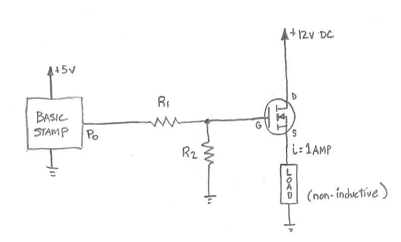
Here is is how I'd like it to work:
When the Stamp output P0 is high, turn on the MOSFET so the +12V DC goes to the load.
When the Stamp output P0 is low, turn the MOSFET off so no power goes to the load.
The load draws 1A, non-inductive. All grounds are common.
Questions are: What type of MOSFET to use (part numbers would be great to know) and are the resistors R1 and/or R2 necessary?
Any other advice on this circuit?
Thanks!
The schematic is shown below. The load must be high side switched.
Here is is how I'd like it to work:
When the Stamp output P0 is high, turn on the MOSFET so the +12V DC goes to the load.
When the Stamp output P0 is low, turn the MOSFET off so no power goes to the load.
The load draws 1A, non-inductive. All grounds are common.
Questions are: What type of MOSFET to use (part numbers would be great to know) and are the resistors R1 and/or R2 necessary?
Any other advice on this circuit?
Thanks!

796 x 481 - 21K
Comments
Easier, would be to use a high-side-switch component. The VN5E160 is such a component that's available for $1.70 qty1 at DigiKey. It will require no components beyond your BASIC Stamp and the load you want to run.
oh, and you maybe should eliminate R1. MOSFETS are turned on by a voltage presence, unlike a bi-polar transistor that is current driven. Depending on the values you used for the transistors, you might switch the FET into it's linear region because the two resistors create a voltage divider - if I understand your circuits' desired operation.
I'd leave R2 as a "fail-safe". It pulls down the gate of the Mosfet and prevents the transistor from turning on should the I/O wire/line from the Stamp become disconnected.
-MattG
Circuitsoft - that chip looks good, but I don't know if we can surface mount in this project. If I switch to P-channel, and invert the Stamp output logic to high=off and low=on, is the second transistor still needed?
feng - thanks for the app note. I've read through it a learned a lot.
Matt - The load must be high side switched. It's a sub-circuit, and can't have a floating ground. I didn't think R1 was necessary, and included R2 as a shutoff if the stamp output is floating. With a P-channel it would become a pull-up instead, right?
Has anyone done this with discrete P-channel MOSFETs I could try to learn from?
Thanks.
-Phil
Almost any P-Chanel MOSFET will work.
Duane J
The additional components R2 and C2 are optional, to control inrush current. Inrush current is important in power supply design when there is a substantial capacitor or incandescent bulb on the output side, not so important for a pure resistive load.
Duane, for Q1, could an NPN transitor work there as well?
Leave R3 at 5K but anything from 1K to 10K would be fine.
R4 is technically not needed in the bipolar circuit but is often used to absorb leakage currents when the micro's pin is in input mode.
Duane J
Sorry, disagree. R1 should be about 180 ohms or thereabouts to protect the microcontroller output from over-current
(MOSFET gates are large capacitive loads, on the order of 5 to 30nF). R2 is a high value, 10k or 100k or so,
to prevent the gate staying charged up when the circuit is off (and thus activating the transistor before the
uController has initialized.
180 / 10k is not going to lose more than a few millivolts as a resistive divider.