

Cramped Delta Sigma PCB Layout
 Duane Degn
Posts: 10,588
Duane Degn
Posts: 10,588
I've been attempting to design some circuit boards to use with the AS5055 magnetic encoder chip.
One of the boards I hope to make would have the encoder chip and a Propeller on a small enough board to fit inside a servo.
I was able to get by with a 2-layer board, but after switching to 4-layers, I found I could fit a few more components onto the board.
I decided to try to fit the passives needed for delta-sigma analog to digital conversions.
Here's what I came up with.

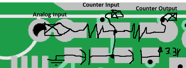
Here's a close up of the delta-sigma section.

I added a (very) rough schematic on top of the board to help indicate the circuit.
I've never tried using a delta-sigma circuit on a PCB before. Does this look like it should work?
Here's the bottom of the board with the Prop.

Counter input is P7 and counter output is P8.
I've read the passive components should be close to the Propeller pins. While the passives in this case are on the other side of the board from the Prop, I'm hoping the components are still close enough to get good ADC readings.
BTW. I included mounting holes for uses other than inside a servo. They would need to be cut off to use inside a servo (I may not include them at all).
Thoughts, comments, critiques?
One of the boards I hope to make would have the encoder chip and a Propeller on a small enough board to fit inside a servo.
I was able to get by with a 2-layer board, but after switching to 4-layers, I found I could fit a few more components onto the board.
I decided to try to fit the passives needed for delta-sigma analog to digital conversions.
Here's what I came up with.
Here's a close up of the delta-sigma section.
I added a (very) rough schematic on top of the board to help indicate the circuit.
I've never tried using a delta-sigma circuit on a PCB before. Does this look like it should work?
Here's the bottom of the board with the Prop.
Counter input is P7 and counter output is P8.
I've read the passive components should be close to the Propeller pins. While the passives in this case are on the other side of the board from the Prop, I'm hoping the components are still close enough to get good ADC readings.
BTW. I included mounting holes for uses other than inside a servo. They would need to be cut off to use inside a servo (I may not include them at all).
Thoughts, comments, critiques?

610 x 637 - 49K
608 x 224 - 17K

595 x 603 - 51K
Comments
Some really nice work there. I look forward to hearing how it performs.
One question I have about the sigma delta circuit... is if one was to do a copper pour under and around the critical 4 or 5 components, would it work better with that copper pour tied to ground, or to the ~1.42v switching threshold (ie the sensing node), or a buffered version of that switching threshold? Haven't had a chance to try it and keep using the MCP3208 by default, but the MCP3208 is a relatively big ic footprint
If we can get that little block working sufficiently well, it might be possible to do an Arduino style host board that used P0..13 for the digitals, and P16..27 to do the 6 analogs using the sigma delta block like you have there, possibly shielded input by input
Wow, fitting in the servo, neat stuff! Congratulations
tubular
Thanks Tubular. It has been fun finally designing some circuit boards; I've wanted to be able to do this for a while.
My PCBs are far from being the artwork yours are.
I'm pretty sure it was your Un3rb3lly board that inspired me to try to make a Propeller board this small.
You're asking me? Heck, the only times I've every used delta-sigma with the Prop is when it's part of a pre-made board using an object written by someone else. In other words, I have no idea what the best pour would be.
I do wonder if using a pour that includes the sensing node would change the capacitance the node experiences compared with only the pair of capacitors. I assume a pour of any sort would add some capacitance to whatever net is connected to the pour.
In this particular case, there isn't enough bare board around the components for much of a pour. I tried a ground pour on the top layer and the pour stayed right around the crystal and the Prop Plug header. There wasn't enough room between traces in other areas of the top layer for a pour to fit.
I do have a 3.3V pour on one inner layer (layer 3) and a ground pour on the an inner layer and the bottom layer.
The MCP3208 is also my ADC of choice. I also use the MCP3002 if I don't need high resolution or many channels since they cost a lot less than the MCP3208.
The Scribbler 2 uses an analog mux to the delta sigma pins on the Prop. I don't know if the mux was used instead of a multichannel ADC because of the cost difference or if using an analog mux provides some other advantage over a separate ADC chip. I suppose an analog mux could be an option for adding ADC channels to the Prop.
I think your congratulations are a bit premature. Let's wait to see if this board can actually do something.
I am excited about these little magnetic encoders. I'm hoping they make building robots easier (and the resulting robots better).
BTW, while the board above is pretty much finished, I do have few tweaks planned for some traces and pads. None of my planned changes will be around the delta sigma components. I will of course make changes to these components if someone points out a way of arranging the components or traces better than their present positions.
Leon, Thanks for taking a look at my board. I'm not sure I know what you are referring to. Is the trace from the circular pad labeled "P20" (lower left of Propeller side of board) to its corresponding Propeller pin what you mean?
I did the same thing with the AS5055 chip on the left side's top and bottom pins. I was trying to get the vias moved to less disruptive locations.
Do you have a suggestion on how to send traces sideways from a pad? Can I make the pad one edge of a big triangular trace?
Like this?
Will the original layout cause signal problems or is it an aesthetics issue?
If you look right above P20 I added a rectangular pad to extend the Prop's P19 pad. I was trying to make it easier to attach a wire to P19 by add some extra copper to solder to. I don't know if I'll really use P19 or not, but I don't like having so many of the Prop's IO pins inaccessible so the thought I'd make them a little easier to solder a wire to them in the few spots I could. I don't have room for full sized pads like P20 gets for the other Propeller pins.
Although, now that I look at it, I might be able to fit a few more P20 sized pads on the board.
Is it just a problem if there's an acute angle between the pad and trace?
What about these other trace/pad connections, are they okay?
Yes, they call that an 'acid trap', and it can undercut a fine trace. Commonly flagged by DFM tools.
Other things to watch for, if you want to eventually automate assembly, is Via-in-pad , as that can wick solder away.
Usually via in pad use micro-via sizes, (or even blind vias) to reduce wicking, and are usually used only as a last resort.
ie when things are so tight, you have no option.
An exception to this, is on large power-pads, where multiple vias can be used as thermals, and we sometimes use paste vias (a via with a solder paste added) for higher current / thermal vias.
Likewise via-between pads - there is one on the Prop.
I can see some vias that seem to go nowhere ? - if they are 'future worm options', they usually have no solder mask ?
I also avoid traces as direct pin-pin bridges, like the SO8 GNDs; Instead I move them under the package, so that ALL pins on the board,
should have clear visual checking - this makes it easier to spot any assembly shorts, as there is NO copper in those places.
Think: 'post assembly visual inspection'.
Leon, Thanks for the advice. I'm making these corrections now. I hope you'll take another look when I post the updated board.
If you see anything else wrong, please let me know. I'm very much a novice at this and I really appreciate your help.
I had wondered about vias inside of a pad. When this was a two layer board, I didn't have much choice on a lot of the vias; I'm not sure I can get rid of all the vias within pads now that I'm using four layers or not, but I'll try.
How much distance from a pad should a via be located? I imagine it would be good to have a line of solder mask between the pad and via. I don't know how thin a line of solder mask could be.
I circled questionable vias in red. Do you think these vias are far enough away from the pads to keep the via from wicking away the solder?
I circled a couple of vias in blue that I think should be okay as is. Am I correct to think these vias are okay?
That's left over from the two layer board. I just couldn't find a place for the via. I've already corrected this problem.
I'm not sure what you are referring to here. There are two layers I haven't posted yet. I'll post them after I finish making the current corrections.
Or do you mean the vias that go to pads (which kind of look like test points)? As I mentioned to Leon, I'm trying to breakout as many unused Propeller pins as I can fit on the board. I'm also trying to breakout all the SPI pins needed to daisy-chain additional encoder only boards to this board.
I've been trying to clean up the way these extra pins are broken out but I doubt I'll get them to look very tidy.
I hadn't thought of this. Is this a common practice or is it a personal preference of yours? I thought know I've seen this done on other PCBs I've seen posted to the forum.
There should be a layer of solder mask on the traces so the pins shouldn't look shorted together.
I have room to move the traces so I move them to under the chip.
Thank you very much for your suggestions.
(ie the solder mask == full annular ring )
Ah, I missed the 4 layer note. In tight designs, it is not a bad idea to go to 4 layer, and then work to remove all possible traces on inner layers, and sometimes you can get it back to 2 layers again... Or you may decide 1 or 2 worms, are less $ than 4Layers.
Both.
It does not flag any DRC checks, but it does improve visual inspection.
If you design to keep clear 'channels' everywhere, ANY blockage is an alert to a problem.
It also means you can easily cut/isolate any single pin, should a modification be needed.
I moved the Propeller chip to one side so there would be room for some full sized holes along one side of the board.
I was able to bring six IO pins out to normal holes and I added solder pads for four more. This should make it easier to use the Prop to control a h-bridge.
I added a segma-delta circuit. One of the capacitors in the sigma-delta circuit is on the bottom of the board.
Here's the top of the board with the AS5055 sensor.
I used a ground pour and the top level and level 2. Do I keep ground a power planes together, or do I alternate between the two on various levels.
The bottom of the board has the Propeller chip.
As I previously mentioned, this is a four layer board. Here's layer two (ground pour).
Here's layer three. It has the 5V line to the regulator. The 5V line is 16mil but it's on an inner layer. I hope that's not a problem. There's also a 3.3V pour on level 3.
I doubt I'll have many of these made, but I think it will be fun to have a Prop inside a servo.
I wasn't able to get a decoupling cap next to each Vdd/Vss pair, but I do have three caps on the 3.3V line. I'm hoping the power and ground planes will help keep the power smooth and clean.
I tried to keep it free from "acid traps".
Once again, I'm hoping for comments.
Thanks for all the help so far.
I'm not sure if this was a good beginner's PCB project.
Of course it was - not much challenge in doing a relay and a transistor
You might want to nudge that crystal a little, as the metal case interferes with a thru-hole.
On pours, I usually move the traces to maximise the floods, and avoid isolated Pour areas.
Also on user-solder connections, thermals make for easier soldering, than flood-over.
On the topic of wire leads, we've seen boards fail at the plating corner, when heavy wires were soldered only on the non-trace-off side.
So now we usually include redundant vias, and teardrops, so that mechanical stress does not have a delicate single point of failure.
The crystal has now been nudged.
Yeah, I didn't notice that until after the pour. I've been scooting traces off to the side so there's more fill area.
I'm guessing a "thermal" is a via that's not require as an electical connection but used to allow heat to pass through to other layers of the board.
I haven't added these yet. I'll likely do this tomorrow. I was a bit worried about the pads peeling off; these "thermals" should help hold them in place.
I think I understand "fail at the plating corner", but "non-trace-off side" leaves me without a quess. Google gives me a bunch of "leave no trace" links. Could you elaborate?
Is this just for the trace mechanical stress or is this also for stress relief to the wires? I don't suppose you have an example you could post or link to?
I'll post updated layouts once I get the pads anchored down with some vias. Before I add the vias, I need to move some traces on the inner layers (since I had moved them to the side to make room for more pour area).
Thanks you very much for your continued help. It's vey much appreciated.
Not quite : Here it is Thermal Relief spokes like on a bicycle wheel, usually + or x and it isolates the solder area thermally from the pour.
Otherwise the heat sucks into the pour, and it takes longer to solder, or you get bad joints.
There are also 'thermal vias' and those are used in multiples to conduct heat. For those we sometimes add paste, to give even more
heat-pathway.
Hehe yes, that was terse - it means the side the trace takes off from - so if you solder on the bottom, and traces come in on the bottom, you are not relying on the plating, but if you have a bare pad on the bottom, and then take traces from top, or inner layers, you are relying on the plating.
If solder wicks all the way through, and you get a top pad fillet, that helps, but you now rely on an operator.
The failures we have seen, are on the thru hole plating, on the side away from the solder, and it is worse with heavier wires.
Hence the addition of redundant vias, and multiple redundant traces.
Where there is room, sometimes we add slots/holes as cable strain relief, ( ie pass the cable thru, before soldering, that takes longer but gives much less stress) but you may not have room for that.
This is one of those things I've often wondered about. I never understood why the little spokes were added when a hole was connected to a pour. I left the spokes on for smt components but I had then turned off for through hole pads. This should be an easy fix.
I've pulled my share of "rings" off of PCB holes. I can see where having a trace connected to the "ring" would give some extra strength.
So if I add multiple traces to a pad, it should make the pad stronger?
I've used these holes many times on the Propeller Protoboard. I don't think I have room for them on this board.
Thanks for the clarifications.
In thinking how to better anchor the solder pads, I'm wondering about adding vias either next to the pad or within the pad. Since these pads aren't used during production (I use the term loosely, since I'll likely use a toaster oven to solder them), I'm thinking the vias within a pad aren't a problem?
I don't like the looks of these extra pads, but I'm pretty sure I'd rather have an ugly looking pad to solder to than trying to solder a wire directly to the leads of the Prop.
Here's an example of a via within a pad I'm considering.
The pad next to the backwards "P27" has a via added where it wont interfere with other layers of the board.
Is this a good idea? I was thinking of adding similar vias to the other pads where there is room on the other other layers for a via to pass through.
Is it better to have such a via in the center, edge, or off to the side, with a small trace, to the pad?
BTW, I've always wanted to do stuff like this (design a PCB), and it's immensely fun (but also very time consuming).
Thanks again for all the help.
The center is always better, as you will get less phone calls from the PCB Fab !!
Offset is not strictly illegal, but I would more likely use an offset oval pad in that case.
If you do use a via, and mask-over vias, then you risk mask bleed thru the via hole, onto the solder area. If that pad was for a test probe, that is a bad thing, and could be another phone call from the PCB fab...
A compromise might be to have two vias, a masked one, and a non-masked one, if your CAD tools can manage that.