

LM10 and its ilk in circuits
 john_s
Posts: 369
john_s
Posts: 369
Tracy,
Thank you for allowing me to open this new thread. I figure it might do good to exchange thoughts related to LM10 and its ilk in circuits. Also, I'd like to pay a small tribute to Robert (Bob) Widlar, Bob Pease and Jim Williams and the amazing amount of designs they left with us.
In various appnotes there are number of circuits applying LM10 in very original and - needles to say - exotic ways. For example, you can single power LM10C and connect its output directly to +40V and still does the job. That feature alone plus many others found its use in the simplest and most elegant 4-20mA transmitters I ever saw.

As I studied the LM10 based 4-20mA circuits (including emesys UCLC) I kept asking myself the following questions:
Q1: How did they arrive with that formula for the output loop current?
Q2: What is the 'save' range of resistor values R1, R2 and R3 in 4-20mA current loop circuit when Vsupply covers an industrial range (say from 9 to 40VDC) ?
Q3: How can I transform a build in 200mV Vref into a Current Source using only a minimal number of additional components yet without touching LM10's op-amp section to the right?
I was informed that the the first question is presented as 'an exercise for the students' during interviews at Linear Technology.
Thanks,
John
Thank you for allowing me to open this new thread. I figure it might do good to exchange thoughts related to LM10 and its ilk in circuits. Also, I'd like to pay a small tribute to Robert (Bob) Widlar, Bob Pease and Jim Williams and the amazing amount of designs they left with us.
In various appnotes there are number of circuits applying LM10 in very original and - needles to say - exotic ways. For example, you can single power LM10C and connect its output directly to +40V and still does the job. That feature alone plus many others found its use in the simplest and most elegant 4-20mA transmitters I ever saw.
As I studied the LM10 based 4-20mA circuits (including emesys UCLC) I kept asking myself the following questions:
Q1: How did they arrive with that formula for the output loop current?
Q2: What is the 'save' range of resistor values R1, R2 and R3 in 4-20mA current loop circuit when Vsupply covers an industrial range (say from 9 to 40VDC) ?
Q3: How can I transform a build in 200mV Vref into a Current Source using only a minimal number of additional components yet without touching LM10's op-amp section to the right?
I was informed that the the first question is presented as 'an exercise for the students' during interviews at Linear Technology.
Thanks,
John
1010 x 457 - 39K
Comments
Let's resolve the values needed for R1 and R2.
Let's assume we have a model for LM10 in a form of LT1635 cousin circuit.
In such case can we say that when R1 = R2 each of them equals at least 50 Ohm? I guess NOT as LTSpice simulation shows that R1 has to be at least equal 100 Ohm alone, otherwise the Vref Voltage Follower above does not work.
Any ideas why the first requirement seems to imply that R1 >= 100 ?
Note: Anything written or drawn above in RED is my imagination and subject to errors waiting to be corrected.
Thanks,
John
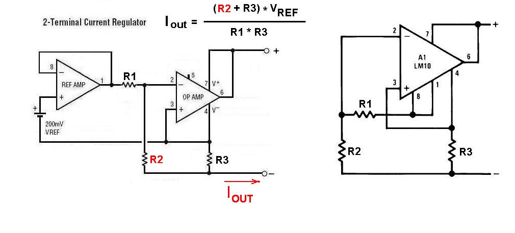
http://circuits.linear.com/p1585-248
from which I borrowed most of the circuit graphics and the following text:
" The LT1635 combines an op amp with a 200mV reference. Scaling this reference voltage to a potential across resistor R3 forces a controlled amount of current to flow from the +terminal to the terminal. Power is taken from the loop. "
Since LT1635 is a younger cousin of LM10 I'd like to concentrate on this circuit as a prime example of an elegant LM10 design.
The question I try to answer remains - how did they come up with that simple formula:
Iout = Vref * (R2+R3) / R1*R3
I'd be glad if forum members with opamp knowledge jump in with help and share their knowledge.
Thanks,
John
Added note: This was in the early 1980's, when tools like SPICE either did not exist or were exotica available only to people with security clearances and eight figure budgets.
Designer of NE555 Hans Camenzind said the following (see http://www.electronicsweekly.com/blogs/engineering-design-problems/2009/03/made-by-masters-3---the-lm10.html)
"The design that has impressed me the most over the years is the National LM10 by Bob Widlar, who else. To me that chip is like a symphony with all the components playing in perfect harmony. We probably won't see anything like that again: it took Widlar five years to design it."
Plus this...
National Semi has always had the most excellent application notes, both standalone an in the data sheets, with description, simplified inner workings at the transistor level, and example application circuits. I hope that continues now that TI bought National for $6.5 billion.
Math:
Choose as reference point the bottom node where Iout exits the circuit.
Notation:
Io will the same as Iout
V3 will be the voltage across R3 with respect to the reference point, also at pin 3 of the op amp.
V2 will be the voltage across R2 wrt the reference point, also at pin 2 of the op amp.
V1 will be the voltage at the output of the reference, the left end of R1.
Vr is the reference voltage. (0.2 V in the LM10)
There is a simple relation between the voltages. Vr is simply stacked on top of V3:
V1 = V3 + Vr
Then there is a simple voltage divider to get from the reference output V1 to the op amp non-inverting input V2:
V2 = V1 * R2 / (R1 + R2)
Put that together and you find,
V2 = (V3 + Vr) * R2 / (R1 + R2)
Now, op amp feedback acts to make V2 = V3. (That is one thing you learn, a rule of thumb that makes solving the basic equations easier). Assume that is true, and later go back and check deeper to see that all the necessary conditions are met for that to be true. Substituting V2 = V3, and then simplifying
V3 = (V3 + Vr) * R2 / (R1 + R2)
V3 = Vr * R2 / R1 <====
The algebra is "left to the reader".
Whoa, where is Io?! It is the sum of two currents, one through R3 and one through R2.
Io = (V3 / R3) + (V2 / R2)
Again, substitute V2 = V3 due to the action of feedback.
Io = V3 * (1/R3 + 1/ R2)
= V3 * (R3 + R2) / (R3 * R2)
Substitute in for V3 the expression marked with <==== above:
Io = (Vr * R2 / R1) * (R3 + R2) / (R3 * R2)
Then simplify (algebra left to the reader!) and viol
Also, the LM10 can source "about 3mA" (see AN-211 page 6) vs 2mA for LT1635
"And since the reference is not included in the thermal protection
control loop, conventional current limit is included on the final
circuit to limit maximum output current to about 3 mA."
Yes, I heard about TI acquiring NS around May this year and it came as a big surprise to an old RCA fellow when I mentioned it to him.
It turns out that the voltage across R1 is always exactly equal to 200 mV. So the reference current is Vr / R1. That is what sets the limit of 200 mV / 100 Ω = 2 mA.
That is exactly the error I kept making in my assumption for ages!
I did not see the obvious that the Vref is dropped across R1.
And that's exactly what LTSpice kept trying to tell me but I still refused to 'see' it.
Simulation went always South when R1 was lower than 100 Ohm, and I was loosing it :-)
Thanks Tracy - I sensed you'd be the one who knew the answer and I kept waiting patiently when you find a moment to jump in and show it with very detailed explanation to all of us 'kids'.
I'm very glad and privileged to be a student in your class!
Thanks,
John
p.s. I guess the op amp feedback that keeps V2=V3 in this case equals Rf = open circuit = approx.infinity, correct?
One similar chip I do use often is the LT6650, which is a reference + op amp in an SOT23-5 package. The 0.4V reference can't be amplified, and is internally tied to the noninverting input of the op amp, but is useful as a configurable voltage source. That chip operates up to 20V and with only 6 µA quiescent current.
>p.s. I guess the op amp feedback that keeps V2=V3 in this case equals Rf = open circuit = approx.infinity, correct?
This circuit does not fit into the mold of the standard inverting and non-inverting op amp circuits, where you have an input resistor and also an Rf feedback resistor. The feedback here occurs because the op amp output is shorted to the + power supply. You can look at the op amp ground terminal (pin 4) through to the power supply (pin 6 and pin 8) as a variable resistor in series with R3, so maybe that can be considered the missing Rf? Does that help?
I was also surprised with lower voltage span for LT1635 (good thing I started playing with just 4xAA batteries :-) although I saw at least one application for 1A current shunt in http://cds.linear.com/docs/Application%20Note/an84f.pdf (author Mitch Lee) that's powered from up to 14.1V, while LT data sheet drops 0.1V from that, and spec shows +/-7V max.
Back to the original circuit - the following can be said about resistor values:
R1(min) = 100 Ohm; limited by Isource(max) = 2mA or "around 3mA" of Vref amplifier only
R1(max) = to meet Iout span expectations
R2(min) = 0
R2(max) = sets Iout(max) that is directly and linearly proportional to R2
R3(min) = to get the Iout(max) yet to NOT exceed Isupply(max) = V+(max) / Iout(max)
R3(max) = to get the Iout(min) of the current loop
I'd be glad to hear any comments on these R values...
Io = Vr * (R2 + R3) / (R1 * R3)
reduces to
Io = Vr * R2 / (R1 * R3)
Most of the current flows through R3. The maximum value of Io should be held to 20mA or less for the LM10, although it can go to 30 or more if power dissipation limits are not exceeded.
Here is a little diagram that shows the circuit as kind of a bridge configuration. The op-amp power path is shown as a variable resistor in series with R3. The op amp output is shorted to the Vdd power supply (don't worry, feedback keeps it from burning out!). The reference is simply a 0.2 volt battery.
Suppose R1 = R2 and R2 >> R3. Under those conditions the equation reduces to, Io = 0.2 / R3. If R3=10Ω, you have a 20mA current source.
What about dynamics of the feedback? When you first turn on the circuit, no current is flowing in R3, but due to the 0.2 volt reference, the voltage on the (-) op amp input will start off higher than the voltage at the (+) input. Specifically, V3 =0 and V2 = 0.1. That causes the op amp to drive its output low, that is, the slider on that op amp power resistor will go toward the low end and the current will build up rapidly through the op amp and R3. Suppose that the op amp overshoots and the voltage across R3 and on the (+) input gets up to 0.4 volt. Then the voltage on the top of R1 input is 0.6 volt, and voltage on the (-) input is one half of that, 0.3 volt. So now the (+) input is 0.1 V higher than the (-) input and that causes the op amp to drive its output high on the slider, increasing that internal resistance and lowering the current. The stable point happens when R1=R2, and R3=10Ω, and the current is 20mA, and at that point the voltage across R3 is equal to the reference, V3 = 0.2 V. The LM10 is internally compensated so overshoots and ringing do not go far over or last long.
1. Can you explain the 10uA current sink limitation of the Vref amp using some sample circuit?
I have a hard time seeing any practical circuit that might try to sink current into the Vref op amp output.
2. How can I transform a build in 200mV Vref into a Current Source using only a minimal number of additional components yet without touching LM10's op-amp section?
Thanks,
John
I think you have a good solution to the current source problem with the reference section of the LM10. I offer a bipolar transistor alternative.
This is technically a current sink, not a source, but the question wasn't all that specific either as to purpose. Your second circuit could work, but you have to add the unregulated 270 µA quiescent current of the LM10, which is a substantial fraction of the 2mA or 3mA max.
Another current source is simply the feedback current, as shown in the following circuit used to generate a linear voltage ramp, charging the capacitor with the constant current. Of course this would need some means to reset the ramp or else it will soon flat top.
Re: the question about the 10 µA sink current for the reference output. I don't think of a specific circuit, but I am sure it could happen. Not just someone trying to turn on an LED as a comparator with current sinking. Voltage regulators and references are typcally source only, and bad things can happen if there is an external circuit forces in current that the regulator and the load on the regulator cannot sink. This is especially true of micropower circuits connected to outside world higher voltage sources. Since the regulator cannot sink the external current, the voltage can rise with bad consequences.
(I'm traveling for a few days--may respond slowly.)
That question had crossed my mind some time ago and I couldn't find an example to prove otherwise. Kind of like what's first - chicken or egg. You have to find a voltage source first to build a current source. Voltage sources exist en mass in nature - where there's a difference of potentials between any bodies or charged particles apart. There's no need for current to flow for the Voltage source to exist.
I invite your comments...
So to build a current source you need a light source. Oh that's a current of photons isn't it...
Another electronic example would be an electrochemical cell carbon monoxide sensor. The current is determined by the rate of reaction, which in turn is determined by the concentration of external gas. To measure that current in the cell, the voltage between two electrodes (reference and working) has to be kept constant, in a circuit called a potentiostat. The LM10 has the basic elements to make a potentiostat, the reference voltage for comparison and the op-amp, with the op-amp output voltage proportional to the cell current.
I was more towards an electric constant voltage source (ECVS) and how you can change it into an equivalent electrical constant current source (ECCS) and vice versa.
From that point of view I can easily identify plenty of ECVS such as charged particles positioned apart from each other, and only AFTER that there's an equivalent ECS when a photo-current, lightning, movements of electrons, photons, molecules etc happens. It seems that the electrical voltage source simply IS i.e. sits still always present dormant yet ready to act, while the electrical current source has to be ACTIVE, i.e has to move, flow, blow, fly, drive....
On a second thought a dead car's battery is an example of EVS-type that IS yet is not ready to act - so I should eliminate any dead 'sources' so to speak :-)
Saying that I accept that my line of thoughts might be totally off or plain wrong, and invite any corrections.
A much better example fluid analogy would be a piston fluid pump, which at a certain speed will have a fixed flow rate regardless of any restrictions -- until you either bog the motor down or blow a gasket.
Tracy,
I'd like to come back a bit to that lovely bipolar current sink alternative circuit, and complement it with some slides that I cut from Bob Pease's video session on "Current Sources and such... ". The whole movie was recorded sometime in 2004 and is available to view on NSC website and else http://www.youtube.com/watch?v=411f0DvXu18&feature=related
Together, those sketches made by RAP form a nice background to what we've discussed so far, and I should have placed them long time ago as the very first topic above all. Well, never too late... and here they are.
Also a question - in the last slide (P7.jpg) Bob gave credits for that design to his coleague Carl Nelson. I tried to locate a source of that simple (yet not frequent in publications) solution to base current compensation and I failed - do you by any chance know that source?
Carl Nelson on Robert Widlar:
"Interaction with Widlar was sometimes not a simple matter. One old friend, Carl Nelson, said, "It was prickly talking to him. Like driving a Ferrari. The car only comes into its own at 150 mph, and things are a little touchy at that speed." ref
I have not used that particular bias compensation circuit, and I confess in looking at it I don't understand how it works. I see it is setting up a bridge configuration, but I'd have to work thru the math in detail and then maybe, maybe there would be an aha! insight. These days, one can use a logic level mosfet in that position and then there is no bias current error to be compensated. I often build the current source with one of the nice Zetex superbeta (~900) bipolar transistors, so the bias current error is pretty small anyway.
Yes, over 500 pages of the very best stuff - I like it. I guess that both text and pics below came from that book... although I'm not sure of the 'simplified LM10' source, as they were captured from some websites.
And to continue on our LM10 constant-current SINK circuit here's another incarnation of it taken from 1998 EDN Design Ideas.
Tracy, I took your simplified version of UCLC and re-drawn it a bit to match our previously discussed layout (I hope you don't mind). I'd like to talk about some component's values and their purpose.
Your original schematic shows Rs = 50 Ohm in series with a photodiode. I guess it's there to set a specific initial reverse photodiode dark current bias to set its optimal working point - correct?
Is it also there to protect an inverting input 8 from excessive photocurrent?
What if to place a jumper across photodiode (i.e to shorten Rs to pin 4) - what can be Rs MIN MAX value in that case?
(I did not show the Zener diode that I guess provides an over-voltage protection to inv.input 8. )
The reference voltage source section of LM10 is configured as inverting amplifier with adjustable gain set by Rf. The photocurrent causes Vr = 0.2V + Is* Rf at pin 1 wrt pin 4.
What is the purpose of R4? Can it be removed? If not, how to calculate R4 MIN and MAX values?
Two equal resistors R1 and R2 (with some help from a little trimmer pot in between) allow to set Iout=4mA when Is=dark current. How to choose R1 and R2 MIN and MAX values?
Thanks,
John
As to R4, it is a pulldown resistor for emitter follower of the reference. The other resistors R1 and R2 also act as pulldowns, but it works better with a little more current. R4 sinks a minimum of about 60 microamps, which is summed into the main feedback path. Beyond that the value is not critical.
Current through resistors R1 and R2 is not included in the main feedback loop, and the equation is simplified when their current is much less than the loop current. However you can see from the equations that their current does not create a gain error. On the low end, they have to be chosen so that it is possible to go down to 4mA total loop current, including the power supply current of the LM10 itself. On the high end, there is the temperature dependence of the LM10 input bias current (-60 pA/°C). Frankly, I have forgotten how I settled on that particular value. It may have involved drift compensation, the negative bias current drift against a positive offset and reference voltage drift. Those parameters vary from batch to batch and within batches. I think the choice of 210k specifically was laughably something very mundane, having a reel of 210k resistors on hand when the boards needed to go out for assembly.
That 'option' made me laugh really hard - I've never thought of that ...
I like your over current (although I must admit seeing it in a kind of 'upside down' fashion for the first time... another WOW!) and over voltage protection plus attention to details in your UCLC design. Excellent design and explanation - thanks.
Just as an add-on for readers - it's worth to mention that probing around this kind of current loop circuit with a scope probe must be limited to fully isolated (battery powered) one, or else...