Using a 74HC165 and a 74HC595 on 4 pins SPIN
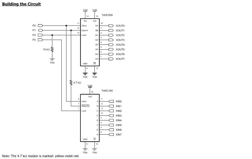
I am having some issues with these shift registers. i have them connected per a drawing found in the Stampworks manual. In this example it shows how to connect the 74HC165 and the 74HC595 to utilize only 4 pins. This is important to me as i only have this many coming from my spinnerett.
The book also provides code for the BS2:
I have also found some code that was written by Michael du Plessis in the object exchange for the Parallax digital I/O board that uses these chips. The problem with this code is that it uses 6 pins and runs the 165 and 595 in seperate cogs.
But i have looked at his code. For the 595
And for the 165
And i have tried to put it together to work on 4 pins. This is what i created, however it does not work.
Any help would be greatly appreciated.
The book also provides code for the BS2:
' {$STAMP BS2}
' {$PBASIC 2.5}
' -----[ Program Description ]---------------------------------------------
'
' This program demonstrates the ability to use the 74HC595 and 74HC165
' together with the fewest number of BASIC Stamp IO pins. This is
' accomplished by placing a 4.7K resistor between the data out (pin 7) of
' the 74HC165 and the data in (pin 14) of the 74HC595. The serial data
' pin from the BASIC Stamp connects to the 74HC595.
' -----[ I/O Definitions ]-------------------------------------------------
Clock PIN 0 ' shift clock
SerData PIN 1 ' serial data (74HC595.14)
Latch PIN 2 ' output latch (74HC595.12)
Load PIN 3 ' input load (74HC165.1)
' -----[ Constants ]-------------------------------------------------------
DelayTime CON 100
' -----[ Variables ]-------------------------------------------------------
xInputs VAR Byte ' external inputs
' -----[ Initialization ]--------------------------------------------------
Reset:
LOW Latch
HIGH Load
DEBUG CLS,
"XInputs 76543210", CR,
"------- --------", CR,
"Status ........"
' -----[ Program Code ]----------------------------------------------------
Main:
DO
GOSUB Get_165 ' get inputs
GOSUB Put_595 ' move to extended outputs
DEBUG CRSRXY, 10, 2, BIN8 xInputs ' display current status
PAUSE DelayTime ' pad the loop a bit
LOOP
' -----[ Subroutines ]-----------------------------------------------------
Get_165:
PULSOUT Load, 5 ' load inputs
SHIFTIN SerData, Clock, MSBPRE, [xInputs] ' shift them in
RETURN
Put_595:
SHIFTOUT SerData, Clock, MSBFIRST, [xInputs] ' send inputs to 595
PULSOUT Latch, 5 ' latch 595 outputs
INPUT SerData ' float data I/O line
RETURN
I have also found some code that was written by Michael du Plessis in the object exchange for the Parallax digital I/O board that uses these chips. The problem with this code is that it uses 6 pins and runs the 165 and 595 in seperate cogs.
But i have looked at his code. For the 595
PUB SHIFTout (SCLK_RLY,LAT_RLY, DATA_RLY,OUT_REG)  |bit    'Call SHIFTout to write a value from an Output Register
repeat
  DIRA[SCLK_RLY]:=%1                                            'into and latch the relays 1-8.
  DIRA[LAT_RLY]:=%1                                             'CLK_RLY is an output
  DIRA[DATA_RLY]:=%1                                            'LAT_RLY is an output
  OUTA[SCLK_RLY]:=0                                             'DATA_RLY is an output
  OUTA[LAT_RLY]:=0                                              'Initialise all to 0
  OUTA[DATA_RLY]:=0

  bit:=BYTE [OUT_REG]
  'bit:=bit<<8
  repeat 8
                                                      'Shift data into 8 bit
    'counter:=counter+1                                                            'Register
    OUTA[DATA_RLY]:=bit                                         '
    bit:=bit>>1                                                 '
    CLOCK (SCLK_RLY)                                            '                                                               'Latch Data into output buffer
  OUTA[LAT_RLY]:=1                                               'Hence operate relays

PUB DELAY                      'slow things down a bit
'waitcnt(cnt+clkfreq/100)      '
return

PUB CLOCK (SCLK_IN)              'Toggle the Clock line
OUTA[SCLK_IN]:=1
'DELAY
OUTA[SCLK_IN]:=0
'DELAY
return
And for the 165
PUB SHIFTin (SCLK_IN,LOAD_IN, DIN,IN_REG_Address) 'Call Shift out to read a value into place holder


  DIRA[SCLK_IN]:=%1
  DIRA[LOAD_IN]:=%1
  DIRA[DIN]:=%0
  inA[DIN]:=0

   OUTA[LOAD_IN]:=1
   CLOCK (SCLK_IN)
repeat
   OUTA[LOAD_IN]:=0
   CLOCK (SCLK_IN)
   OUTA[LOAD_IN]:=1
   'bit:=bit<<8
   REPEAT 8
     bit:=bit<<1
     bit|=inA[DIN]
     CLOCK (SCLK_IN)
     'DELAY

  bit:=bit
  byte[IN_REG_Address]:=bit


PUB DELAY                      'slow things down a bit
'waitcnt(cnt+clkfreq/100)      '
return

PUB CLOCK (SCLK_IN)              'Toggle the Clock line
OUTA[SCLK_IN]:=1
'DELAY
OUTA[SCLK_IN]:=0
'DELAY
return
And i have tried to put it together to work on 4 pins. This is what i created, however it does not work.
PUB SHIFT (CLK,LATCH, DATA,LOAD,OUT_REG,IN_REG_Address)  |bit    'Call SHIFTout to write a value from an Output Register
repeat
  DIRA[CLK]:=%1                                            'into and latch the relays 1-8.
  DIRA[LATCH]:=%1                                             'CLK_RLY is an output
  DIRA[DATA]:=%1                                            'LAT_RLY is an output
  OUTA[CLK]:=0                                             'DATA_RLY is an output
  OUTA[LATCH]:=0                                              'Initialise all to 0
  OUTA[DATA]:=0

  bit:=BYTE [OUT_REG]
  'bit:=bit<<8
  repeat 8
                                                      'Shift data into 8 bit
    'counter:=counter+1                                                            'Register
    OUTA[DATA]:=bit                                         '
    bit:=bit>>1                                                 '
    CLOCK (CLK)                                            '                                                               'Latch Data into output buffer
  OUTA[LATCH]:=1                                               'Hence operate relays


  DIRA[CLK]:=%1
  DIRA[LOAD]:=%1
  DIRA[DATA]:=%0
  inA[DATA]:=0

   OUTA[LOAD]:=1
   CLOCK (CLK)

   OUTA[LOAD]:=0
   CLOCK (CLK)
   OUTA[LOAD]:=1
   'bit:=bit<<8
   REPEAT 8
     bit:=bit<<1
     bit|=inA[DATA]
     CLOCK (CLK)
     'DELAY

  bit:=bit
  byte[IN_REG_Address]:=bit
Any help would be greatly appreciated.


Comments
For the 165:
Pin 15 (Clock Inhibit) must be tied low.
P0 (clock) must be low.
P1 on the prop must be set as an input pin. P0, P2, P3 must be outputs.
P3 must go low to load the parallel data to the shift register.
P3 must go high to permit data to be shifted by the clock signal.
Repeat 8 times per 165 in chain:
Input the data from P1 ( pin 7 of the 165 is the inverted, pin 9 is non inverted data ).
P0 goes from low to high and back to low to shift data 1 bit position.
For the 595:
Pin 13 (/G) must be tied low.
Pin 10 (/SRCLR) must be pulled high.
P0 (clock) must be low.
On the prop P0, P1, P2, P3 must be outputs.
Repeat 8 times per 595 in chain:
Output the data to P1.
P0 goes from low to high and back to low to shift serial data 1 bit position.
P2 must go high, then low to load the data from the serial register to the output register.