The output \input transistor must be somehow set to create these impedances. I have redrawn the circuit to include what I think is correct. (attached drawing)
Thanks and Regards
Bob (WRD)
BTW, MOSFETs have a large number of possible constructions. Representing them all in one symbol hasn't be uniformly adopted. I've seen three different ways to draw an enhancement mode N-channel MOSFET:
The original symbol has an arrow for the diodic junction from substrate to the middle of the channel. N-type pointing inward, P-type pointing outward.
The above example shows an arrow for current flow from positive to negative on the source pin.
Will switch to Mosfet for digital (I think I know what to do) but the current source I was wondering if you could sketch a top and bottom current source and I will reproduce in drawing. I kind of follow what you are saying. When I was learning everything was bipolar NPN or PNP biased transistors.
Regards and Thanks
Bob (WRD)
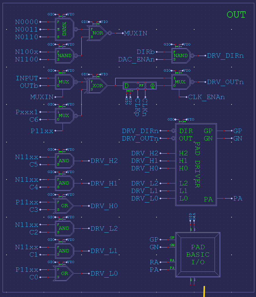
I'll also point out that there is more parts to the low-level I/O. Not just an optional inversion. Here's the glue sections for each:
Output: The upper half of image is the output source select which are OUT or Input feedback, then inversion, then registering. Plus separate DIR handling:
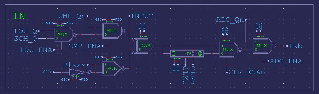
Input: Sources here are Logic input, Schmitt input, Comparator input, then feedback [to output], then inversion, then registering, then another select for ADC [bitstream] input:
Man, I just freaked out when I discovered I'd deleted a bunch of my reference files! I had been accidentally pressing delete key while the picture viewer was selected instead of the schematic entry window. I belatedly realised this was deleting each image from the drive!
Luckily, being a desktop aware viewer, it was actually moving those files to the trashcan instead of fully deleting them.
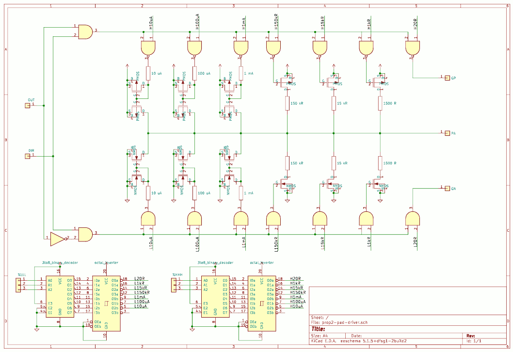
PS: For the 3to8 binary decoders, I've used 74LS138 parts. They're not correct for the use (Shouldn't have inverted outputs) but I was too lazy to draw my own.
EDIT: Updated the drawing by adding an octal inverter to correct for the 74LS138's inverted outputs.
That drawing has a lot of detail and effort, thanks for detailing the current source. I think a lot of people will find this very useful. I would like to include this in my notes and
replace what is existing. I am using digikey schema free software. Is KiCad a free software? Should I add xor for M6M7 Input Output Inversion or is this done differently and is
whole lot more complicated. Losing software stuff, been there and really done it.
Regards and Thanks
Bob (WRD)


Comments
No. The pin drive circuits are active only. There is no passive pull-up/dn resistors.
To make a pull-up, you config the pin mode for the chosen pull-up strength,15k, then drive it high as an output.
The output \input transistor must be somehow set to create these impedances. I have redrawn the circuit to include what I think is correct. (attached drawing)
Thanks and Regards
Bob (WRD)
Yep, getting better.") However, some fixes:
However, some fixes:
Where would the resistors go ?
Regards and Thanks
Bob (WRD)
Excellent. Oops, I missed the fact you've used JFET symbols rather than MOSFET symbols. Should change those too.
I'll dig up a current control circuit ... here we go, courtesy of https://www.allaboutcircuits.com/technical-articles/the-basic-mosfet-constant-current-source/
So, what you do is drive Rset from the OUT control instead of attached to Vdd. And Vcs is attached to the pin output.
That's the low side drive. The high side is flipped over, using P-type mosfets.
BTW, MOSFETs have a large number of possible constructions. Representing them all in one symbol hasn't be uniformly adopted. I've seen three different ways to draw an enhancement mode N-channel MOSFET:
Will switch to Mosfet for digital (I think I know what to do) but the current source I was wondering if you could sketch a top and bottom current source and I will reproduce in drawing. I kind of follow what you are saying. When I was learning everything was bipolar NPN or PNP biased transistors.
Regards and Thanks
Bob (WRD)
Getting the hang of KiCAD ...
I'll also point out that there is more parts to the low-level I/O. Not just an optional inversion. Here's the glue sections for each:
Output: The upper half of image is the output source select which are OUT or Input feedback, then inversion, then registering. Plus separate DIR handling:
Input: Sources here are Logic input, Schmitt input, Comparator input, then feedback [to output], then inversion, then registering, then another select for ADC [bitstream] input:
Man, I just freaked out when I discovered I'd deleted a bunch of my reference files! I had been accidentally pressing delete key while the picture viewer was selected instead of the schematic entry window. I belatedly realised this was deleting each image from the drive!
Luckily, being a desktop aware viewer, it was actually moving those files to the trashcan instead of fully deleting them.")
Righty-oh, one guessed at "pad driver" schematic:
PS: For the 3to8 binary decoders, I've used 74LS138 parts. They're not correct for the use (Shouldn't have inverted outputs) but I was too lazy to draw my own.
EDIT: Updated the drawing by adding an octal inverter to correct for the 74LS138's inverted outputs.
That drawing has a lot of detail and effort, thanks for detailing the current source. I think a lot of people will find this very useful. I would like to include this in my notes and
replace what is existing. I am using digikey schema free software. Is KiCad a free software? Should I add xor for M6M7 Input Output Inversion or is this done differently and is
whole lot more complicated. Losing software stuff, been there and really done it.
Regards and Thanks
Bob (WRD)
Sure is - https://www.kicad.org/
That's fine, it's that way in the glue snippet I posted yesterday. Here's the low level pin-pad schematic that Chip posted: (Shows how all those M bits are used) - https://forums.parallax.com/discussion/comment/1494131/#Comment_1494131
Here's a 3to8 binary decoder without the baggage of extra inverters and enables: (Combination arrangement courtesy of OnSemi datasheet for 74LS138)

And a Logisim simulator version attached also
This is the latest revision. Added Call instructions , COGEXEC\HUBEXEC files and some general corections.
PropellerP2NotesDocuments
Regards
Bob (WRD)
Latest Revision 13 added spin2 command section
Regards
Bob (WRD
HelloPropellerP2Rev13
Thank you Bob!
Thanks Bob!