Looks like the P2 chip or the software is the reason for it, not the board and that's good to know .
To be honest, I suspected it from the start when you described the problem but I'm glad I kept my mouth shut until now. I'll test my KISS boards this weekend too.
EDIT: ok, I saw the post in the KISS thread ten seconds ago - looks like it's even better. The software can be corrected/polished far more easy than the silicon.
@Scroungre said:
Better! But not quite perfect... I cut and pasted your "PRI computeClockMode(desiredHz)" code and replaced the old method with that, and it ran happily up to about 348MHz before complaining about a 'set RAM Delay failed'. See attached text.
Error -6 is invalid arguments (ERR_INVALID). Looks like the delay parameter calculation it tries to make is invalid but it's weird because this means the parameter values passed are bad or some other data structure corruption. Maybe some HUB RAM accesses start getting corrupted at that high a frequency?
' method to set the delay value used in the driver for the memory device mapped to the address
' addr - address of the Hyper device to configure
' delay - nibble value passed is (delayClocks * 2) + (registeredDataBusFlag)
' returns 0 for success or negative error code
PUB setDelay(addr, delay) : r
    if delay +> 15
        return ERR_INVALID
    r := modifyBankParams(addr, $FFFF0FFF, delay << 12)


' internal method modifies the bank specific parameters for the given addr and applies to the driver
PRI modifyBankParams(addr, andmask, ormask) : r | bus, bank, value, size, i, m
    bus := addrMap[addr >> 28]
    if bus +> LAST_INSTANCE
        return ERR_INVALID

    ' driver must be running
    if driverCogs[bus] == -1
        return ERR_INACTIVE

    ' get starting bank and size used by this address
    bank := getStartBank(bus, addr)
    if bank < 0
        return ERR_INVALID
    size := devices[bus * 2 * NUMBANKS + bank] & $ff

    m := mailboxAddr[bus] + driverCogs[bus]*12
    repeat until LOCKTRY(driverlock)
    ' configure parameter(s) over all spanned banks and update local storage also
    repeat i from bank to bank + ((1<<(size - S_16MB)) - 1)
        value := (devices[bus * 2 * NUMBANKS + i] & andmask) | ormask
        long[m][1] := value
        long[m] := R_SETPARAMS + (i<<24) + cogid()
        repeat
            r := long[m]
        until r >= 0
        if r == 0
            devices[bus * 2 * NUMBANKS + i] := value
        else ' error case
            r := -r
            quit ' TODO: cleanup?, potentially leaves multi-banks in an inconsistent state

    LOCKREL(driverlock)
@Scroungre said:
The PLL code (with the con block and the Compute Clock method results gave me exactly the same results as yours. (at 25MHz Xtal). S.
PS - For grinsies, I tested out my other KISS (I had bought two) and lightly tweaked your PLL calculation numbers to run up to 360MHz. It did. See attached...
Ok so it is working now with this code, or do you still see failures in the delay test using this code? EDIT: just read your other results. Looks like it works now. Why it failed before at 301MHz is a mystery though unless my posted PLL calculation code above was different from yours. I took it from the release 0.8 zip.
@evanh said:
Most likely a software bug me thinks. Scroungre using the driver in unexpected way or something.
Maybe. I can't make my version fail that way, so perhaps a compiler difference, or something else Scroungre might have modified causing it. Until I hear of some way to definitively reproduce this I will be assuming my code is okay for now.
Hm. Yeah, it does seem I've gotten behind the curve again on compilers - will update that.
It's possible I've screwed it up - I know just enough spin2 to be dangerous with it. The "PLL" results were from your code in post 899, just to replicate those results - which I then edited a few numbers to see what it would get me at 360MHz, which I did.
I will have to have a think about what happens at 348MHz in the memory read/write test when it tries to pick another delay.
The code worked beautifully 'out-of-the-box' on my 20MHz Xtal P2 edge, even if the memory access was Smile. Now I have a much better memory bus, but the code's giving me trouble. I'll bang on it a bit more on my own. Thanks much for putting all this energy into it for me. 's appreciated. S.
The 348MHz issue might be indicating a hub RAM corruption issue at that high a clock speed. I've not seen this in my setup when I test up to 350MHz. An invalid parameter error indicates something being passed or checked has a problem and is out of range. The COG mailbox is typically not even accessed at that point so it is not the driver COG failing to respond. I wonder if hub RAM read access is failing or something is getting corrupted in hub memory at that frequency. You could always modify your memory.spin2 to print out the reason when it finds the error in setDelay() or modifyBankParams(), getStartBank() etc. Just call SPIN2's send() method where it happens and print the memory contents etc. To me it looks like data corruption of delay or addrMap that would do that.
I'll have a go at it, but given my history of screwing things up, I'm not entirely enthusiastic about the idea. But it's the least I can do - your code did present intelligent error codes, which is more than I can say for some! I'll poke around quite a bit more on my end. S.
In time for the holidays I have just released an updated memory driver package (version 0.9b) now containing my PSRAM driver and some initial support for SRAM (experimental), as well as a few demos and tools showing what it can do, including frame buffer graphics that work with my video driver. Check it out in the first post of this thread.
It has been primarily been tested with flexspin (5.9.3) and also some in PropellerTool (both 2.6.0 and 2.5.3).
Just wrapped up the coding of a 4 bit PSRAM driver variant and am about to start testing it. This was MUCH simpler than the 16 bit variant and easier to fit in the COG as well. The memory addressing now matches the native storage size of the device so there is no need to read-modify-write all the various cases where individual bytes/words get written in longs (as was needed for the 16 bit variant used by the new P2 Edge board).
Once this testing work is done I'll update the driver suite to include it. It should be useful for simple single PSRAM device setups with just 6 P2 pins. This includes my own Voyager board. Even though it has one quarter of the bandwidth and size as a 4 PSRAM device setup it should be able to provide sufficient bandwidth for simple 8bpp VGA and SVGA video frame buffers with VGA or HDMI outputs, or lower depths. If we're lucky, maybe even XGA @ 8bpp (DAC only) when the P2 is pushed to 325MHz, probably only with aligned 1kB blocks per scan line. TBD.
In this single device configuration the raw memory bandwidth equals the P2 frequency / 4 MB/s.
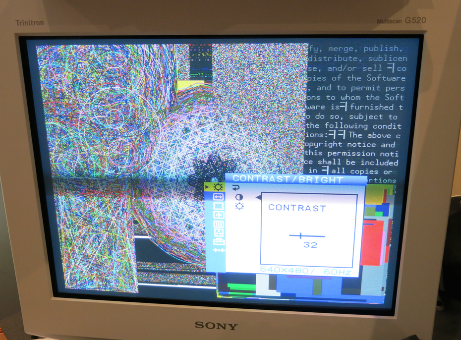
My 4 bit PSRAM (single chip) driver seems to be working with VGA now. Still testing but happy to see this working already. P2 is running at 252MHz here. PSRAM is clocking out nibbles at 126MHz (or 63MB/s).
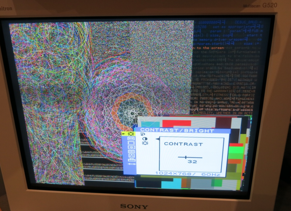
Wow, SVGA and XGA also work at 8bpp. Neat! P2 is at 325MHz below.
Ignore the ghosted text, the screen was updating rapidly while I took the photo.
@rogloh said:
My 4 bit PSRAM (single chip) driver seems to be working with VGA now. Still testing but happy to see this working already. P2 is running at 252MHz here. PSRAM is clocking out nibbles at 126MHz (or 63MB/s).
Based on this, whether or not multiple PSRAM chips are needed would often depend on size, not speed. How many MB in one chip?
@pik33 said:
Is it restricted to clock/2 ? (I am thinking about 320/3..
Right now my code does a divide by 2 only but you could probably try to tweak the timing in the driver to try to experiment with that. Not too sure about the duty cycle for the divide by 3 clock, hopefully it would work although the data sheet says it should be in the 45-55% range. I was thinking about adding a divide by 4 option sometime in the future for people who didn't want to overclock their PSRAM at all.
Perhaps I'm losing something, but, up to the extent of my knowledge, the ways one can resort, in order to craft a "Sysclk/3" output-signal by using the smart pins (e.g.: mode %00100 = pulse/cycle output), meant to drive, says, the clock signal for external Ram chips(s), would result in a 33/66 duty cycle (or 66/33), whichever best fits, in order to ensure stable data in/out, to/from the Rams.
@Fred777 said:
Is there perhaps any chance of a single chip PSRAM (beta??) driver soon? - doesn't have to be polished...
Yeah I have been busy on other stuff lately but here's a quick sample you can play with until the proper release if you are really keen. I've provided a simple VGA demo that works with it too based off an earlier demo provided in the latest official release - you should use the same P2 video driver from that zip. It seems to work ok but this code was not well tested as I've paused working on it for a few weeks while doing other things so you may find issues...but hopefully not. It also includes a couple of ported graphics functions from the main driver which is still a work in progress. I have been accelerating the text rendering too but that part was removed for clarity as it was incomplete.
You may also need to tweak the memory delay timings if you encounter data corruption at different frequencies because the frequency breakpoints will likely be different for your board vs the P2 Edge implementation. This is because your wire length and impedances will be different. My psram_delay_test SPIN2 program is useful for measuring this, but still needs to be adjusted to work with the 4 bit driver as it currently works with the larger memory driver API which still defaults to the 16 bit PSRAM version only. If you are handy in SPIN2 you may be able to make the adjustments required for that, as I think it might only be a couple of lines of patching driver names/parameters...? Otherwise I'll need to take a look soon to see what else is needed there with the API changes to officially try to support the 4 bit driver variant alongside the existing 16 bit version.
I had been waiting for this version too. I prepared 1 and 4 chip breakout boards - 1 chip version is much more easy to (hardware) debug and run, including soldering this to 12 pin connector for Eval board.8 MB is big enough capacity for Amiga modules, offline framebuffers and a lot of other useful stuff.
Yeah the one chip variant is handy for pin limited setups and 8MB is still quite a lot of memory, although the bandwidth is just 25% of the P2 Edge 32MB so a single chip can only burst around 70-85MB/s peak or so depending on P2 clock rate, and this is without factoring in the extra access overheads. For video frame buffer applications you'll have to limit the colour depth or resolution somewhat, but I've managed to get 1024x768 at 8bpp IIRC. Four chips has significantly more performance for video.
Actually yeah it should be 4 * n. That constant was left over from the P2Edge. I should test this variant for ensuring it can operate on a 4 * n port boundary...I think it should but haven't tried yet. UPDATE: I just tried it out and it worked on either 40, 44, 48, 52 with the P2 Edge 32MB (which has 4 devices but this driver is only using one of them).
Just noticed in my rush to get out the last zip file with the 4 bit PSRAM demo I still had this code commented out below...I expect it can cause problems as the demo code appears to now be using an uninitialized variable called cogBurstLimit. It still appears to work with my FlexSpin build but that is not guaranteed at all. I think I'd commented out this calculation as it could fail with the slower 4 bit PSRAM (which has a 4x smaller burst size in the maximum 8uS CS low time interval).
{
    ' TODO: fix this for 4 bit PSRAM driver stuff...

    cogBurstLimit := mem.getBurst() - XSIZE*((BPP+7)/8) - MARGIN
    if cogBurstLimit < 0
        DEBUG("No write bandwidth left for reliable video")
        repeat
}
I'll try to look today at the real changes needed there but to work around it in the meantime if you have problems you could play about with the cogBurstLimit limit to be something like 64 or 128 or 256 bytes at VGA resolutions for example and find something that works. For higher resolutions and bit depths it would be likely be less. This parameter actually sets up the maximum number of bytes that the writer COGs can transfer in one go and you need to keep the value small enough to fit within the remaining bandwidth per scan line after the video COG takes its fill of the bandwidth which varies with resolution/video timing/P2 timing and bit depth...so it can't be fixed and gets more complicated to compute.
Took a look, this is getting more complicated. The full max burst calculation pseudocode seems to be something like this, and I still need to determine what the transfer_overhead_clocks value is:
p2_clocks_per_scanline = total_pixels_per_scan_line * p2_clocks_per_pixel
device_burst_size = (((MAX_CS_LOW_USEC*(p2_frequency/4000000)) - 132) >> 4) << 4 ' for 4 bit PSRAM device with 8uS !CS low time max
max_transfer_size = MIN(device_burst_size, configured_burst_size_for_video_cog)
total_video_bytes_per_scanline = roundup(active_pixels_per_scanline * bits_per_pixel / 8)
num_video_transfers = roundup(total_video_bytes_per_scanline / max_transfer_size)
p2_clocks_per_byte = 4 ' this is 4 for a single PSRAM, or 1 for 16 bit PSRAM array
p2_clocks_per_video_transfer = (num_video_transfers * transfer_overhead_clocks) + total_video_bytes_per_scanline * p2_clocks_per_byte
available_clocks_for_other_cogs = p2_clocks_per_scanline - p2_clocks_per_video_transfer
low_priority_cog_burst_size <= (available_clocks_for_other_cogs - 132 ) / p2_clocks_per_byte - MARGIN ' where MARGIN is a safety margin
Real code could be something like this...
PRI computeBurst(timing) : cogburst | scanline_clks, burst, video_transfers, active_pixels, video_clks, video_bytes, available_clks
    active_pixels := byte[timing+8] * 8 ' get active pixels from columns in video mode timing
    scanline_clks := active_pixels
    scanline_clks += byte[timing+9]  ' add BP blanking pixels
    scanline_clks += byte[timing+10] ' add sync pixels
    scanline_clks += byte[timing+11] & $7f  ' add FP blanking pixels
    scanline_clks *= byte[timing+13]  ' NOTE: this ONLY supports integer clocks for now
    burst := mem.getBurst()  ' get device's maximum allowed burst size
    video_bytes := (active_pixels * BPP) / 8 ' compute number of bytes needed to be transferred per scanline
    video_transfers := (video_bytes + (burst-1)) / burst ' figure out how many fragments will be sent
    video_clks := (video_transfers * OVERHEAD) + video_bytes * 4 ' compute P2 clocks per video scan line
    available_clks := scanline_clks - video_clks ' compute remaining clocks
    cogburst := (available_clks - 132) / 4 - MARGIN ' transform into bytes allowed to be transferred
    cogburst &= !$f ' quantize transfer to a 16 byte multiple
    if (cogburst < 0)
        return 0
I've updated the prior 4 bit PSRAM video demo code to now include this type of more accurate burst timing computation - I've tested it with 1024x768 and it appears to work for that resolution. Note this graphics demo is only coded to support 8bpp. It's still not perfect because not all driver timing values have been accurately measured at this point but it's a start and has a better chance of working than the old implementation did.
With a 4 bit PSRAM you get enough bandwidth to get XGA, SVGA and VGA working.


Comments
Looks like the P2 chip or the software is the reason for it, not the board and that's good to know") .
.
To be honest, I suspected it from the start when you described the problem but I'm glad I kept my mouth shut until now. I'll test my KISS boards this weekend too.
EDIT: ok, I saw the post in the KISS thread ten seconds ago - looks like it's even better. The software can be corrected/polished far more easy than the silicon.
Error -6 is invalid arguments (ERR_INVALID). Looks like the delay parameter calculation it tries to make is invalid but it's weird because this means the parameter values passed are bad or some other data structure corruption. Maybe some HUB RAM accesses start getting corrupted at that high a frequency?
' method to set the delay value used in the driver for the memory device mapped to the address ' addr - address of the Hyper device to configure ' delay - nibble value passed is (delayClocks * 2) + (registeredDataBusFlag) ' returns 0 for success or negative error code PUB setDelay(addr, delay) : r if delay +> 15 return ERR_INVALID r := modifyBankParams(addr, $FFFF0FFF, delay << 12) ' internal method modifies the bank specific parameters for the given addr and applies to the driver PRI modifyBankParams(addr, andmask, ormask) : r | bus, bank, value, size, i, m bus := addrMap[addr >> 28] if bus +> LAST_INSTANCE return ERR_INVALID ' driver must be running if driverCogs[bus] == -1 return ERR_INACTIVE ' get starting bank and size used by this address bank := getStartBank(bus, addr) if bank < 0 return ERR_INVALID size := devices[bus * 2 * NUMBANKS + bank] & $ff m := mailboxAddr[bus] + driverCogs[bus]*12 repeat until LOCKTRY(driverlock) ' configure parameter(s) over all spanned banks and update local storage also repeat i from bank to bank + ((1<<(size - S_16MB)) - 1) value := (devices[bus * 2 * NUMBANKS + i] & andmask) | ormask long[m][1] := value long[m] := R_SETPARAMS + (i<<24) + cogid() repeat r := long[m] until r >= 0 if r == 0 devices[bus * 2 * NUMBANKS + i] := value else ' error case r := -r quit ' TODO: cleanup?, potentially leaves multi-banks in an inconsistent state LOCKREL(driverlock)Ok so it is working now with this code, or do you still see failures in the delay test using this code? EDIT: just read your other results. Looks like it works now. Why it failed before at 301MHz is a mystery though unless my posted PLL calculation code above was different from yours. I took it from the release 0.8 zip.
Most likely a software bug me thinks. Scroungre using the driver in unexpected way or something.
Maybe. I can't make my version fail that way, so perhaps a compiler difference, or something else Scroungre might have modified causing it. Until I hear of some way to definitively reproduce this I will be assuming my code is okay for now.
Hm. Yeah, it does seem I've gotten behind the curve again on compilers - will update that.
It's possible I've screwed it up - I know just enough spin2 to be dangerous with it. The "PLL" results were from your code in post 899, just to replicate those results - which I then edited a few numbers to see what it would get me at 360MHz, which I did.
I will have to have a think about what happens at 348MHz in the memory read/write test when it tries to pick another delay.
The code worked beautifully 'out-of-the-box' on my 20MHz Xtal P2 edge, even if the memory access was Smile. Now I have a much better memory bus, but the code's giving me trouble. I'll bang on it a bit more on my own. Thanks much for putting all this energy into it for me. 's appreciated. S.
The 348MHz issue might be indicating a hub RAM corruption issue at that high a clock speed. I've not seen this in my setup when I test up to 350MHz. An invalid parameter error indicates something being passed or checked has a problem and is out of range. The COG mailbox is typically not even accessed at that point so it is not the driver COG failing to respond. I wonder if hub RAM read access is failing or something is getting corrupted in hub memory at that frequency. You could always modify your memory.spin2 to print out the reason when it finds the error in setDelay() or modifyBankParams(), getStartBank() etc. Just call SPIN2's send() method where it happens and print the memory contents etc. To me it looks like data corruption of delay or addrMap that would do that.
I'll have a go at it, but given my history of screwing things up, I'm not entirely enthusiastic about the idea. But it's the least I can do - your code did present intelligent error codes, which is more than I can say for some! I'll poke around quite a bit more on my end. S.
To push the limits puts you into the risk to be pushed by the Limits😊
In time for the holidays I have just released an updated memory driver package (version 0.9b) now containing my PSRAM driver and some initial support for SRAM (experimental), as well as a few demos and tools showing what it can do, including frame buffer graphics that work with my video driver. Check it out in the first post of this thread.
It has been primarily been tested with flexspin (5.9.3) and also some in PropellerTool (both 2.6.0 and 2.5.3).
Just wrapped up the coding of a 4 bit PSRAM driver variant and am about to start testing it. This was MUCH simpler than the 16 bit variant and easier to fit in the COG as well. The memory addressing now matches the native storage size of the device so there is no need to read-modify-write all the various cases where individual bytes/words get written in longs (as was needed for the 16 bit variant used by the new P2 Edge board).
Once this testing work is done I'll update the driver suite to include it. It should be useful for simple single PSRAM device setups with just 6 P2 pins. This includes my own Voyager board. Even though it has one quarter of the bandwidth and size as a 4 PSRAM device setup it should be able to provide sufficient bandwidth for simple 8bpp VGA and SVGA video frame buffers with VGA or HDMI outputs, or lower depths. If we're lucky, maybe even XGA @ 8bpp (DAC only) when the P2 is pushed to 325MHz, probably only with aligned 1kB blocks per scan line. TBD.
In this single device configuration the raw memory bandwidth equals the P2 frequency / 4 MB/s.
My 4 bit PSRAM (single chip) driver seems to be working with VGA now. Still testing but happy to see this working already. P2 is running at 252MHz here. PSRAM is clocking out nibbles at 126MHz (or 63MB/s).
Wow, SVGA and XGA also work at 8bpp. Neat! P2 is at 325MHz below.
Ignore the ghosted text, the screen was updating rapidly while I took the photo.
Based on this, whether or not multiple PSRAM chips are needed would often depend on size, not speed. How many MB in one chip?
Commonly available serial (QPI) parts are up to 8 MB.
Is it restricted to clock/2 ? (I am thinking about 320/3... 960x540x8bpp needs about 32 MB/s... ) I have prepared a contraption with P2 Edge and a breakout board (this: https://www.parallax.com/product/p2-edge-80-pin-adapter-kit/ ) - I have several memory chips and these boards: https://botland.com.pl/przejsciowki-smd-dip/2742-przejsciowka-sop-na-dip-8-pin-10szt-5904422303907.html - I think about soldering the PSRAM to this board, and then solder this directly to the Edge adapter kit with as short connection as I can do....
Right now my code does a divide by 2 only but you could probably try to tweak the timing in the driver to try to experiment with that. Not too sure about the duty cycle for the divide by 3 clock, hopefully it would work although the data sheet says it should be in the 45-55% range. I was thinking about adding a divide by 4 option sometime in the future for people who didn't want to overclock their PSRAM at all.
Perhaps I'm losing something, but, up to the extent of my knowledge, the ways one can resort, in order to craft a "Sysclk/3" output-signal by using the smart pins (e.g.: mode %00100 = pulse/cycle output), meant to drive, says, the clock signal for external Ram chips(s), would result in a 33/66 duty cycle (or 66/33), whichever best fits, in order to ensure stable data in/out, to/from the Rams.
Yeah @Yanomani that can be done, but it will violate the data sheet specs for clock signal duty cycle. Whether that matters in practice is TBD.
Having single chip PSRAM support would be very helpful, I have exactly 6 free pins and need memory for my project.
Great stuff!
Is there perhaps any chance of a single chip PSRAM (beta??) driver soon? - doesn't have to be polished...
Yeah I have been busy on other stuff lately but here's a quick sample you can play with until the proper release if you are really keen. I've provided a simple VGA demo that works with it too based off an earlier demo provided in the latest official release - you should use the same P2 video driver from that zip. It seems to work ok but this code was not well tested as I've paused working on it for a few weeks while doing other things so you may find issues...but hopefully not. It also includes a couple of ported graphics functions from the main driver which is still a work in progress. I have been accelerating the text rendering too but that part was removed for clarity as it was incomplete.
You may also need to tweak the memory delay timings if you encounter data corruption at different frequencies because the frequency breakpoints will likely be different for your board vs the P2 Edge implementation. This is because your wire length and impedances will be different. My psram_delay_test SPIN2 program is useful for measuring this, but still needs to be adjusted to work with the 4 bit driver as it currently works with the larger memory driver API which still defaults to the 16 bit PSRAM version only. If you are handy in SPIN2 you may be able to make the adjustments required for that, as I think it might only be a couple of lines of patching driver names/parameters...? Otherwise I'll need to take a look soon to see what else is needed there with the API changes to officially try to support the 4 bit driver variant alongside the existing 16 bit version.
I had been waiting for this version too. I prepared 1 and 4 chip breakout boards - 1 chip version is much more easy to (hardware) debug and run, including soldering this to 12 pin connector for Eval board.8 MB is big enough capacity for Amiga modules, offline framebuffers and a lot of other useful stuff.
Yeah the one chip variant is handy for pin limited setups and 8MB is still quite a lot of memory, although the bandwidth is just 25% of the P2 Edge 32MB so a single chip can only burst around 70-85MB/s peak or so depending on P2 clock rate, and this is without factoring in the extra access overheads. For video frame buffer applications you'll have to limit the colour depth or resolution somewhat, but I've managed to get 1024x768 at 8bpp IIRC. Four chips has significantly more performance for video.
85 MB/s? It is way more than I expected from 4bit 133 MHz chip") Does it mean the chip works at 170 MHz?
Does it mean the chip works at 170 MHz?
Overclocked...yeah. See pics above of this working at 1024x768.
Where to get this from?
And another question:
DATABUS = 40Is it 4n or 8n?
I didn't include in this zip but you can get it from within the latest release 0.9b zip file here...
https://forums.parallax.com/discussion/171176/memory-drivers-for-p2-psram-sram-hyperram-was-hyperram-driver-for-p2
Actually yeah it should be 4 * n. That constant was left over from the P2Edge. I should test this variant for ensuring it can operate on a 4 * n port boundary...I think it should but haven't tried yet. UPDATE: I just tried it out and it worked on either 40, 44, 48, 52 with the P2 Edge 32MB (which has 4 devices but this driver is only using one of them).
Just noticed in my rush to get out the last zip file with the 4 bit PSRAM demo I still had this code commented out below...I expect it can cause problems as the demo code appears to now be using an uninitialized variable called cogBurstLimit. It still appears to work with my FlexSpin build but that is not guaranteed at all. I think I'd commented out this calculation as it could fail with the slower 4 bit PSRAM (which has a 4x smaller burst size in the maximum 8uS CS low time interval).
{ ' TODO: fix this for 4 bit PSRAM driver stuff... cogBurstLimit := mem.getBurst() - XSIZE*((BPP+7)/8) - MARGIN if cogBurstLimit < 0 DEBUG("No write bandwidth left for reliable video") repeat }I'll try to look today at the real changes needed there but to work around it in the meantime if you have problems you could play about with the cogBurstLimit limit to be something like 64 or 128 or 256 bytes at VGA resolutions for example and find something that works. For higher resolutions and bit depths it would be likely be less. This parameter actually sets up the maximum number of bytes that the writer COGs can transfer in one go and you need to keep the value small enough to fit within the remaining bandwidth per scan line after the video COG takes its fill of the bandwidth which varies with resolution/video timing/P2 timing and bit depth...so it can't be fixed and gets more complicated to compute.
Took a look, this is getting more complicated. The full max burst calculation pseudocode seems to be something like this, and I still need to determine what the transfer_overhead_clocks value is:
Real code could be something like this...
PRI computeBurst(timing) : cogburst | scanline_clks, burst, video_transfers, active_pixels, video_clks, video_bytes, available_clks active_pixels := byte[timing+8] * 8 ' get active pixels from columns in video mode timing scanline_clks := active_pixels scanline_clks += byte[timing+9] ' add BP blanking pixels scanline_clks += byte[timing+10] ' add sync pixels scanline_clks += byte[timing+11] & $7f ' add FP blanking pixels scanline_clks *= byte[timing+13] ' NOTE: this ONLY supports integer clocks for now burst := mem.getBurst() ' get device's maximum allowed burst size video_bytes := (active_pixels * BPP) / 8 ' compute number of bytes needed to be transferred per scanline video_transfers := (video_bytes + (burst-1)) / burst ' figure out how many fragments will be sent video_clks := (video_transfers * OVERHEAD) + video_bytes * 4 ' compute P2 clocks per video scan line available_clks := scanline_clks - video_clks ' compute remaining clocks cogburst := (available_clks - 132) / 4 - MARGIN ' transform into bytes allowed to be transferred cogburst &= !$f ' quantize transfer to a 16 byte multiple if (cogburst < 0) return 0I've updated the prior 4 bit PSRAM video demo code to now include this type of more accurate burst timing computation - I've tested it with 1024x768 and it appears to work for that resolution. Note this graphics demo is only coded to support 8bpp. It's still not perfect because not all driver timing values have been accurately measured at this point but it's a start and has a better chance of working than the old implementation did.
With a 4 bit PSRAM you get enough bandwidth to get XGA, SVGA and VGA working.