Ok, well it should be available very soon. In the meantime I can provide you with a test app binary that can interactively test your SRAM setup at different P2 speeds and on different pins. Let me try to get that together in the next couple of hours...
Yes it is designed for other purposes such as audio or storage use too in parallel with video. Because QoS is built into the design with video getting priority over other accesses, it can share the memory bandwidth nicely with other lower priority COGs. You could setup some of the external memory for a temporary FAT filesystem for example and make it available to other COG(s). Someone here has already started looking into doing just that...
As well as future PSRAM, we also have the HyperFlash support as well for a filesystem to use. Its reads operate even faster than the HyperRAM (over ~300MB/s) but it's writes are obviously much slower, under 1MB/s IIRC. The sector erase time is the main killer there. But for a (mostly) read-only filesystem and for storing large amounts of static lookup data that needs to be accessed quickly by the P2, it's a great match.
@aaaaaaaargh If you'd like to mess about with some alpha grade binaries for testing with your SRAM here's a zip file with some new stuff in it.
All output to the console port at 115200bps. Use Loadp2 to load the binaries.
1) sramdelay.binary
This is a tool that lets you find out the required input delay for a given frequency. It scans through the range and reads random data to see if it matches for different delay values. My slow RAM tops out at 40MHz so I couldn't try it higher to setup the default timing profile, but yours might if you have faster RAM and better signal integrity. My delay test result output is shown below (EDIT: damn column formatting got messed up):
2) sramvideo.binary
This is a small graphics drawing demo that can output Y/C + Composite on the A/V board, or VGA and reads from external RAM. It works perfectly with both PSRAM and HyperRAM without issues however I see lots of bad pixel noise/corruption in my dodgy SRAM breadboard setup but maybe you might be luckier. The VGA output is really bad too and shaky. As a result I still don't know if this is a hidden bug remaining in the driver setup or flaky signal integrity etc. So it will be good to know if it works any better for you. I need to make a PCB with the SRAM for proper timing testing.
This video code is clocking the P2 really slowly at 40.5MHz for NTSC and 50MHz for VGA so that it can read from my own slow SRAM and the memory read rate is half of this so the performance is not amazing. A faster P2 clock and some faster SRAM timing would obviously improve this.
At the end of the test loop runs you get a portion of a Mario image shown from HUB RAM for comparison of stability. That's how it should look from SRAM too if things were working right (but they are not for me).
3) sramtest.binary
This binary lets you interactively trigger data transfers to/from external SRAM and HUB. It lets you fill, copy, dump, compare etc. You can also setup transfers to loop continually until a key is pressed, for probing timing on an oscilloscope etc. The "Scratch" memory is a 64kB area of HUB RAM to safely play with, without corrupting the application if you remain within its range.
All three binaries let you specify the SRAM pins. The address bus pins must be contained within a single port (A or B ), while the others can be put anywhere (but the data bus needs to be aligned to a group of 8 pins). I recently changed the address bus to make it more flexible but that is poorly tested as yet. Most of my tests were with the address bus starting at port A P0 pin. The pin defaults I use all come up in the output on the console but can be overridden if your setup is different.
See how you go...there is not much support here as this is alpha for the SRAM part. I've included the source for two of these diagnostic test binaries so you can see what they do if you run into issues (code's a bit rough and needs more tidying) but not the driver's source yet as it's not 100% ready.
Hope it whets your appetite...it'll be good if/when it works right.
@rogloh, thanks very much, alas my P2 board has a 25Mhz smd crystal (P2KISS board) and I havent been brave enough to change it to a 20Mhz one yet as it is so tiny... so all the console output is garbled as it comes out at 115200x1.25 bps or so... I have to set 184320bps instead of 240300 and 92160bps instead of 115200 to get the console working... or fiddle with clock divider settings...
Very nice results for a breadboard. Better than what I have with my poor old SRAM chip. I need to make a PCB with some fast SRAM.
The reason your VGA is jittery is probably because I am running the P2 a bit too slow. If I could run it at 100MHz I think the jitter would go away. With NTSC output does it look stable? And do you get static pixel corruption like I did or is the image clean with NTSC? You get composite video on one pin and Y/C on two other pins when you choose this output type.
@aaaaaaaargh said:
VGA Test is running - output looks a bit jittery or like its interlaced, but promising! And there is Mario!
Hopefully the P2KISS board you are using does not suffer from the P28-P31 problem with it's crystal input pin being affected. I noticed you are using P24 for your data bus, which would normally be bad on a P2-EVAL and a P2-EDGE and cause VGA jitter. The test code allows P24 even though it is not listed in the set of values.
@aaaaaaaargh Here's a new SRAM video demo binary that will run the P2 @ 75MHz instead of 50MHz and the RAM at 37.5MB/s which is enough for 8bpp VGA plus some write bandwidth left over. It should fix your jitter issue over VGA. I built it for your 25MHz crystal. You may need to tweak your delay value to suit the best image output.
One thing I noticed in my own breadboard setup is there is a LOT of noise getting on the video output and sync pins. Crosstalk is appearing during high speed data transfers when the address/data buses are actively switching. It's really not an ideal setup. A proper PCB layout with SRAM should improve that significantly.
Great, thanks the jitter is gone!
Still a lot of breadboard noise in the picture, there are some "bad pixels" visible during circle and box drawing - they always appear in the same locations distributed along a vertial line.
I have moved the SRAM Data Port to pin 32 and the VGA to 24 - it doesn't look like there is any difference on the screen but i get better results when doing ram write/read/verify speed tests
The "bad pixels" existed before the switch at the same locations...
So maybe down to the P24 issue or just different cabling conditions now - can't tell with breadboard ;-)
Sorry, I don't have any device that does ntsc - all digital here...
Yeah these static pixels may be cross talk from the address bus getting into the data bus somehow. Certain transitions might possibly result in reading bad pixel data. That's my guess anyway.
We both need some PCB based SRAM I believe to improve the integrity.
Is there some information about the P28-31 issue? I have moved to P32 for the SRAM Data Port but can P28-31 even be reliably used for other things? e.g. VGA output. I have noticed far higher error rates when testing the SRAM at high clock frequencies with simple bit banging - making me think my board may also be affected
I'm looking forwards to testing it! One thing I can agree with you so far on is:
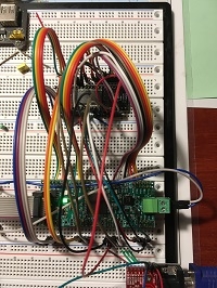
Breadboarding SRAM is a pain in the keester!!
And I'm not sure I started my SRAM address pins on an eight-bit pin boundary. I may still have to move a wire or two. The data bus, however, is straight! (The address pins are completely scrambled, partially because I found out very late I'd skipped a pin on the data bus, and had to rearrange quite a few wires!). I am using P28 and other local pins as address - I hope they won't be a problem. For now, I don't need fast (what I need is two ring buffers in each cog, but I'm working on that too).
@aaaaaaaargh said:
Is there some information about the P28-31 issue?
The issue is switching noise injection into the crystal oscillator causing PLL instability onto the system clock. I don't think it affects reliability of the Prop2, or at least it doesn't when the PLL is engaged, but can throw timing issues with external devices that need stable syncs like video signals.
There is some debate as to how the switching noise of the P28-P31 I/O group is reaching into the oscillator but it does require the FAST drive strength and multiple pins switching the same polarity in parallel. It has documented effect with the Eval and Edge boards. P2D2 and RetroBlade2 don't exhibit the symptoms. A notable commonality in layouts is the tight spacing of XI and XO tracks on the Eval and Edge boards.
@Scroungre said:
I'm looking forwards to testing it! One thing I can agree with you so far on is:
Breadboarding SRAM is a pain in the keester!!
And I'm not sure I started my SRAM address pins on an eight-bit pin boundary. I may still have to move a wire or two. The data bus, however, is straight! (The address pins are completely scrambled, partially because I found out very late I'd skipped a pin on the data bus, and had to rearrange quite a few wires!). I am using P28 and other local pins as address - I hope they won't be a problem. For now, I don't need fast (what I need is two ring buffers in each cog, but I'm working on that too).
Testing SRAM code next! S.
Your wiring is a lot tidier and shorter than mine so hopefully it might help reduce the noise a bit. I've recently changed the code to allow the address bus to start on any P2 pin (so long as they don't cross port A/B boundary). It did cost two instructions in the accesses to copy and shift the start address but I think it is worth it for the flexibility so I put it in. You need to be careful about what follows the address bus though as that pin can also potentially get driven high on the final transfer. Safest to have P31 as the last address pin, or the CE signal for the memory because that pin will rise then anyway and be cleared to zero on the next transfer so address wraparounds won't propagate to even higher port bits.
If you don't run fast, and the P28-P31 pins are upper address bits which change less, you may not see a problem with the PLL variation.
By the way I'm also creating a "HUB" SRAM driver. This is useful so we can use HUB RAM to emulate external RAM for software debug/testing purposes without real HW fitted.
Several banks of powers of 2 sized memory blocks can be mapped as usual like real HW would be, at different HUB RAM addresses. I've also coded it to try to approximately emulate sysclk/1 read speeds, and sysclk/2 write speeds, similar to what HyperRAM delivers. It simply slots into my memory driver framework like the other memory types do, so applications can be developed before final HW is ready.
Obviously you wouldn't need this extra layer if you were going to always use internal memory but it may still be handy in some situations.
Yeah it's handy to do this. Here's a binary for the 20MHz systems that anyone can load to show the test running without needing external SRAM but just reading from HUBRAM emulating HyperRAM. The A/V breakout base pin is selectable. Needs 115200 bps on the console.
There are some visual boundary artifacts due only a 64kB block of external RAM being emulated in this particular case. Too much of the remaining HUB RAM was taken up by the bitmap image.
Also for some reason loadp2 does not like loading the larger sized binaries to the P2 Edge via the PropPlug. This binary is close to 512k and I get lots of download timeouts on a Mac (~40%). But not with the P2-EVAL for some weird reason and I don't know why. Different FTDI chip settings on these two setups maybe?
I am using loadp2 v0.047. Also noticed that the PropPlug resets the P2 Edge board when you exit the terminal, whilst the P2-EVAL does not reset the board when you exit the terminal. Maybe that has something to do with it.
@Scroungre said:
I'm looking forwards to testing it! One thing I can agree with you so far on is:
Breadboarding SRAM is a pain in the keester!!
And I'm not sure I started my SRAM address pins on an eight-bit pin boundary. I may still have to move a wire or two. The data bus, however, is straight! (The address pins are completely scrambled, partially because I found out very late I'd skipped a pin on the data bus, and had to rearrange quite a few wires!). I am using P28 and other local pins as address - I hope they won't be a problem. For now, I don't need fast (what I need is two ring buffers in each cog, but I'm working on that too).
Testing SRAM code next! S.
Your wiring is a lot tidier and shorter than mine so hopefully it might help reduce the noise a bit. I've recently changed the code to allow the address bus to start on any P2 pin (so long as they don't cross port A/B boundary). It did cost two instructions in the accesses to copy and shift the start address but I think it is worth it for the flexibility so I put it in. You need to be careful about what follows the address bus though as that pin can also potentially get driven high on the final transfer. Safest to have P31 as the last address pin, or the CE signal for the memory because that pin will rise then anyway and be cleared to zero on the next transfer so address wraparounds won't propagate to even higher port bits.
If you don't run fast, and the P28-P31 pins are upper address bits which change less, you may not see a problem with the PLL variation.
For now, I have my highest address pin on P31 - but P32 is the start of the data bus. Hope that won't be a problem. The SRAM is only rated to 4.5V - We'll find out if it behaves at 3.3, because I'm not sure the P2 has 5V tolerant input pins.
I don't intend to run this one particularly fast, especially given the undervoltage spec. It's rated to 15ns /CE to 'Data Valid', and 7ns /OE same, but at 4.5V. Mostly it's just 'proof o' concept'.
In short, it's a disaster area - but I sorta expected that!
It does seem to work fairly consistently at 64MHz and a 'delay' of (5). 24MHz and (4) got consistent 100%s too. Oddly enough, going slower made it worse - It bopped around the high 80s to 90% between 4MHz and 25, but 10% RAM errors is not quite acceptable!
Anything over 80MHz got flat 0% correct, throughout.
So some work needs to be done yet. I need to build a proper SRAM board, use SRAMs rated for 3.3V, and all that. I'm hoping to run the P2 at 350 internally, and have delays for the external RAM..
Anyhow, heap good fun trying it! Thanks for your code! S.
In case anyone cares, I put here the complete speed tests. Unfortunately, the more sophisticated RAM tests gave weird results - possibly due to me using them wrong - so I don't have much for you there.
The .spin2 code didn't even want to compile (where's variable 'f'?). The binaries seemed to have address issues (off by one? Off by a lot more? Trying to put in "0A" "0A"s got me nine of them, and perhaps it's expecting a 64k SRAM? Mine's only 32... &c.)
Also the website scripts get weird and starting timing out. Hardly our problem here, but it does make me a titch grumpy while posting. Anyhow: S.
@Scroungre said:
For now, I have my highest address pin on P31 - but P32 is the start of the data bus. Hope that won't be a problem. The SRAM is only rated to 4.5V - We'll find out if it behaves at 3.3, because I'm not sure the P2 has 5V tolerant input pins.
P31 should be okay for upper addresses, if your board doesn't have the XI/PLL issue or you don't toggle them at high rates. P32-39 is good for data. The 5V part might not give a fast slew rate when rising to a logic high level. I noticed that with my undervolted SRAM on the scope.
It does seem to work fairly consistently at 64MHz and a 'delay' of (5). 24MHz and (4) got consistent 100%s too. Oddly enough, going slower made it worse - It bopped around the high 80s to 90% between 4MHz and 25, but 10% RAM errors is not quite acceptable!
Yes this is a strange result. It might be your 5V SRAM operating at 3.3V and its signal integrity is not that good. One thing I did was reduce the actual test pattern copy size so I could run the tests at slower frequencies in a timely way. When I increased it more tests actually failed.
Anything over 80MHz got flat 0% correct, throughout.
Yes that would be really pushing it on a breadboard.
So some work needs to be done yet. I need to build a proper SRAM board, use SRAMs rated for 3.3V, and all that. I'm hoping to run the P2 at 350 internally, and have delays for the external RAM..
Yes same here. For faster P2 speeds the SRAM code needs to be modified to add some wait state support which is not in my driver yet.
The .spin2 code didn't even want to compile (where's variable 'f'?). The binaries seemed to have address issues (off by one? Off by a lot more? Trying to put in "0A" "0A"s got me nine of them, and perhaps it's expecting a 64k SRAM? Mine's only 32... &c.)
I only provided the binaries so you wouldn't be able to compile it. The included source was just to show how the diagnostic test itself worked. If the address is off by a byte or two it might be the delay needs adjustment for your operational frequency. I'm not sure about the 0A thing unless you encountered foldover in memory. It was setup for a 2MB SRAM.
Also the website scripts get weird and starting timing out. Hardly our problem here, but it does make me a titch grumpy while posting. Anyhow: S.
Yeah I know and feel the pain acutely too. No one seems to know why the forum server is having so many problems or how to fix it AFAIK. This short post has taken me 10 mins to type in, and I've had to click "Wait" about 20 times when "A web page is slowing down your browser" in Firefox. You can probably type about 3-10 chars before it kicks in again. Best to type into a separate editor first and paste the whole thing.
I only provided the binaries so you wouldn't be able to compile it. The included source was just to show how the diagnostic test itself worked. If the address is off by a byte or two it might be the delay needs adjustment for your operational frequency. I'm not sure about the 0A thing.
Yeah, I didn't look too hard at that. Alpha software - If I don't like, I can get my money back, huh?
If you want me to beaver away more carefully at that I could probably get you some better diagnostic information, but I don't think it's real important right now. Suffice to say that data can be written and read back out - That's what we're trying to find out here, and it does!
Thanks again for all this stuff. It makes the world better. S.
PS - Thanks for letting me know it's not just me having forum software trouble. S.
Everyone complained about the bugginess when Parallax adopted the new forum software. Apparently the old stable software wasn't supported by developers any longer. Probably because it worked too well.
Sort of forcing Parallax to change to the buggy stuff that now needs fixed.
@rogloh said:
Yeah these static pixels may be cross talk from the address bus getting into the data bus somehow. Certain transitions might possibly result in reading bad pixel data. That's my guess anyway.
We both need some PCB based SRAM I believe to improve the integrity.
I noticed that I get VGA noise even when no cables and SRAM are connected. I was writing 2M of random Data to the 2M SRAM (Adr = P0-P20, P21,22,33 for chip control and P32-P39 for Data) with nothing but the vga cable connected. Chaning the VGA port doensn't make a difference. Oh dear, maybe the Noise is picked up from the board or maybe in the prop itself?
That doesn't sound good. But breadboards are hardly noise free setups. When I scoped my bus activity and the video output I could see plenty of noise getting onto the video pins very easily during the time of the memory transfers and it was also visible on the LCD monitor. Even you don't have any wires connected the P2 signal is still attached to those metal breadboard channels attached to the address/data bus pins. A proper circuit board is the way to go for video frequencies and when you have fast IO transitions.
Your right of course, i pulled the board from the breadboard with only vga and power connections and without the breadboard "antenna" the vga noise is gone... Well, then a pcb it must be...


Comments
Ok, well it should be available very soon. In the meantime I can provide you with a test app binary that can interactively test your SRAM setup at different P2 speeds and on different pins. Let me try to get that together in the next couple of hours...
Yes it is designed for other purposes such as audio or storage use too in parallel with video. Because QoS is built into the design with video getting priority over other accesses, it can share the memory bandwidth nicely with other lower priority COGs. You could setup some of the external memory for a temporary FAT filesystem for example and make it available to other COG(s). Someone here has already started looking into doing just that...
As well as future PSRAM, we also have the HyperFlash support as well for a filesystem to use. Its reads operate even faster than the HyperRAM (over ~300MB/s) but it's writes are obviously much slower, under 1MB/s IIRC. The sector erase time is the main killer there. But for a (mostly) read-only filesystem and for storing large amounts of static lookup data that needs to be accessed quickly by the P2, it's a great match.
@aaaaaaaargh If you'd like to mess about with some alpha grade binaries for testing with your SRAM here's a zip file with some new stuff in it.
All output to the console port at 115200bps. Use Loadp2 to load the binaries.
1) sramdelay.binary
This is a tool that lets you find out the required input delay for a given frequency. It scans through the range and reads random data to see if it matches for different delay values. My slow RAM tops out at 40MHz so I couldn't try it higher to setup the default timing profile, but yours might if you have faster RAM and better signal integrity. My delay test result output is shown below (EDIT: damn column formatting got messed up):
2) sramvideo.binary
This is a small graphics drawing demo that can output Y/C + Composite on the A/V board, or VGA and reads from external RAM. It works perfectly with both PSRAM and HyperRAM without issues however I see lots of bad pixel noise/corruption in my dodgy SRAM breadboard setup but maybe you might be luckier. The VGA output is really bad too and shaky. As a result I still don't know if this is a hidden bug remaining in the driver setup or flaky signal integrity etc. So it will be good to know if it works any better for you. I need to make a PCB with the SRAM for proper timing testing.
This video code is clocking the P2 really slowly at 40.5MHz for NTSC and 50MHz for VGA so that it can read from my own slow SRAM and the memory read rate is half of this so the performance is not amazing. A faster P2 clock and some faster SRAM timing would obviously improve this.
At the end of the test loop runs you get a portion of a Mario image shown from HUB RAM for comparison of stability. That's how it should look from SRAM too if things were working right (but they are not for me).
3) sramtest.binary
This binary lets you interactively trigger data transfers to/from external SRAM and HUB. It lets you fill, copy, dump, compare etc. You can also setup transfers to loop continually until a key is pressed, for probing timing on an oscilloscope etc. The "Scratch" memory is a 64kB area of HUB RAM to safely play with, without corrupting the application if you remain within its range.
All three binaries let you specify the SRAM pins. The address bus pins must be contained within a single port (A or B ), while the others can be put anywhere (but the data bus needs to be aligned to a group of 8 pins). I recently changed the address bus to make it more flexible but that is poorly tested as yet. Most of my tests were with the address bus starting at port A P0 pin. The pin defaults I use all come up in the output on the console but can be overridden if your setup is different.
See how you go...there is not much support here as this is alpha for the SRAM part. I've included the source for two of these diagnostic test binaries so you can see what they do if you run into issues (code's a bit rough and needs more tidying) but not the driver's source yet as it's not 100% ready.
Hope it whets your appetite...it'll be good if/when it works right.
SRAM memory read delay test over frequency, ESC exits Enter the base data pin number for your SRAM (0,8,16,32,40,48) [48]: 48 Enter the base address pin number for your SRAM [0]: 0 Enter the chip enable pin number for your SRAM [21]: 21 Enter the write enable pin number for your SRAM [22]: 22 Enter the output enable pin number for your SRAM [23]: 23 Enter a starting frequency to test in MHz (4-350) : [50] 4 Enter the ending frequency to test in MHz (4-350) : [350] 50 Enter 1 to use the automatic delay value only, or 0 to test over the delay range : [0] 0 Enter 1 to display the first error encountered, or 0 to not display error details : [0] 0 Testing P2 from 4000000 - 50000000 Hz Successful data reads from 100 block transfers of 256 random bytes Frequency Delay 3 4 5 6 7 8 9 10 11 12 13 14 4 MHz (4) 100% 100% 0% 0% 0% 0% 0% 0% 0% 0% 0% 0% 5 MHz (4) 100% 100% 0% 0% 0% 0% 0% 0% 0% 0% 0% 0% 6 MHz (4) 100% 100% 0% 0% 0% 0% 0% 0% 0% 0% 0% 0% 7 MHz (4) 100% 100% 0% 0% 0% 0% 0% 0% 0% 0% 0% 0% 8 MHz (4) 100% 100% 0% 0% 0% 0% 0% 0% 0% 0% 0% 0% 9 MHz (4) 100% 100% 0% 0% 0% 0% 0% 0% 0% 0% 0% 0% 10 MHz (4) 100% 100% 0% 0% 0% 0% 0% 0% 0% 0% 0% 0% 11 MHz (4) 100% 100% 0% 0% 0% 0% 0% 0% 0% 0% 0% 0% 12 MHz (4) 100% 100% 0% 0% 0% 0% 0% 0% 0% 0% 0% 0% 13 MHz (4) 100% 100% 0% 0% 0% 0% 0% 0% 0% 0% 0% 0% 14 MHz (4) 0% 100% 0% 0% 0% 0% 0% 0% 0% 0% 0% 0% 15 MHz (4) 0% 100% 0% 0% 0% 0% 0% 0% 0% 0% 0% 0% 16 MHz (4) 0% 100% 0% 0% 0% 0% 0% 0% 0% 0% 0% 0% 17 MHz (4) 0% 100% 0% 0% 0% 0% 0% 0% 0% 0% 0% 0% 18 MHz (4) 0% 100% 0% 0% 0% 0% 0% 0% 0% 0% 0% 0% 19 MHz (4) 0% 100% 0% 0% 0% 0% 0% 0% 0% 0% 0% 0% 20 MHz (4) 0% 100% 0% 0% 0% 0% 0% 0% 0% 0% 0% 0% 21 MHz (4) 0% 100% 0% 0% 0% 0% 0% 0% 0% 0% 0% 0% 22 MHz (4) 0% 100% 0% 0% 0% 0% 0% 0% 0% 0% 0% 0% 23 MHz (4) 0% 100% 3% 0% 0% 0% 0% 0% 0% 0% 0% 0% 24 MHz (4) 0% 100% 100% 0% 0% 0% 0% 0% 0% 0% 0% 0% 25 MHz (4) 0% 100% 100% 0% 0% 0% 0% 0% 0% 0% 0% 0% 26 MHz (5) 0% 100% 100% 0% 0% 0% 0% 0% 0% 0% 0% 0% 27 MHz (5) 0% 100% 100% 0% 0% 0% 0% 0% 0% 0% 0% 0% 28 MHz (5) 0% 94% 100% 0% 0% 0% 0% 0% 0% 0% 0% 0% 29 MHz (5) 0% 47% 100% 0% 0% 0% 0% 0% 0% 0% 0% 0% 30 MHz (5) 0% 0% 100% 0% 0% 0% 0% 0% 0% 0% 0% 0% 31 MHz (5) 0% 0% 100% 0% 0% 0% 0% 0% 0% 0% 0% 0% 32 MHz (5) 0% 0% 100% 0% 0% 0% 0% 0% 0% 0% 0% 0% 33 MHz (5) 0% 0% 100% 0% 0% 0% 0% 0% 0% 0% 0% 0% 34 MHz (5) 0% 0% 100% 0% 0% 0% 0% 0% 0% 0% 0% 0% 35 MHz (5) 0% 0% 100% 0% 0% 0% 0% 0% 0% 0% 0% 0% 36 MHz (5) 0% 0% 100% 0% 0% 0% 0% 0% 0% 0% 0% 0% 37 MHz (5) 0% 0% 100% 0% 0% 0% 0% 0% 0% 0% 0% 0% 38 MHz (5) 0% 0% 100% 0% 0% 0% 0% 0% 0% 0% 0% 0% 39 MHz (5) 0% 0% 92% 0% 0% 0% 0% 0% 0% 0% 0% 0% 40 MHz (5) 0% 0% 76% 0% 0% 0% 0% 0% 0% 0% 0% 0% 41 MHz (5) 0% 0% 26% 0% 0% 0% 0% 0% 0% 0% 0% 0% 42 MHz (5) 0% 0% 2% 0% 0% 0% 0% 0% 0% 0% 0% 0% 43 MHz (5) 0% 0% 0% 0% 0% 0% 0% 0% 0% 0% 0% 0% 44 MHz (5) 0% 0% 0% 0% 0% 0% 0% 0% 0% 0% 0% 0% 45 MHz (5) 0% 0% 0% 0% 0% 0% 0% 0% 0% 0% 0% 0% 46 MHz (5) 0% 0% 0% 0% 0% 0% 0% 0% 0% 0% 0% 0% 47 MHz (5) 0% 0% 0% 0% 0% 0% 0% 0% 0% 0% 0% 0% 48 MHz (5) 0% 0% 0% 0% 0% 0% 0% 0% 0% 0% 0% 0% 49 MHz (5) 0% 0% 0% 0% 0% 0% 0% 0% 0% 0% 0% 0% 50 MHz (5) 0% 0% 0% 0% 0% 0% 0% 0% 0% 0% 0% 0%@rogloh, thanks very much, alas my P2 board has a 25Mhz smd crystal (P2KISS board) and I havent been brave enough to change it to a 20Mhz one yet as it is so tiny... so all the console output is garbled as it comes out at 115200x1.25 bps or so... I have to set 184320bps instead of 240300 and 92160bps instead of 115200 to get the console working... or fiddle with clock divider settings...
Ok I've tried a quick recompile for a 25MHz crystal, and have posted the updated zip here (but it will be untested)....
Thanks ever so much, looks like the setup is good at 100Mhz and Delay 5: incredible speed with that cable mess...
Enter the base data pin number for your SRAM (0,8,16,32,40,48) [48]: 24 (*** HAVE used P24 although it is not listed as an option, is this because of the Edge Board Data corruption issue?) Enter the base address pin number for your SRAM [0]: 0 Enter the chip enable pin number for your SRAM [21]: 21 Enter the write enable pin number for your SRAM [22]: 22 Enter the output enable pin number for your SRAM [23]: 23 Enter a starting frequency to test in MHz (4-350) : [50] 50 Enter the ending frequency to test in MHz (50-350) : [350] 150 Enter 1 to use the automatic delay value only, or 0 to test over the delay range : [0] 0 Enter 1 to display the first error encountered, or 0 to not display error details : [0] 0 Testing P2 from 50000000 - 150000000 Hz Successful data reads from 100 block transfers of 256 random bytes Frequency Delay 3 4 5 6 7 8 9 10 11 12 13 14 50 MHz (5) 81% 100% 0% 0% 0% 0% 0% 0% 0% 0% 0% 0% 51 MHz (5) 91% 100% 0% 0% 0% 0% 0% 0% 0% 0% 0% 0% 52 MHz (5) 96% 100% 0% 0% 0% 0% 0% 0% 0% 0% 0% 0% 53 MHz (5) 99% 100% 0% 0% 0% 0% 0% 0% 0% 0% 0% 0% 54 MHz (5) 97% 100% 0% 0% 0% 0% 0% 0% 0% 0% 0% 0% 55 MHz (5) 100% 100% 0% 0% 0% 0% 0% 0% 0% 0% 0% 0% 56 MHz (5) 99% 100% 0% 0% 0% 0% 0% 0% 0% 0% 0% 0% 57 MHz (5) 100% 100% 0% 0% 0% 0% 0% 0% 0% 0% 0% 0% 58 MHz (5) 100% 100% 0% 0% 0% 0% 0% 0% 0% 0% 0% 0% 59 MHz (5) 100% 100% 0% 0% 0% 0% 0% 0% 0% 0% 0% 0% 60 MHz (5) 100% 100% 0% 0% 0% 0% 0% 0% 0% 0% 0% 0% 61 MHz (5) 100% 100% 0% 0% 0% 0% 0% 0% 0% 0% 0% 0% 62 MHz (5) 81% 100% 0% 0% 0% 0% 0% 0% 0% 0% 0% 0% 63 MHz (5) 16% 100% 0% 0% 0% 0% 0% 0% 0% 0% 0% 0% 64 MHz (5) 0% 100% 0% 0% 0% 0% 0% 0% 0% 0% 0% 0% 65 MHz (5) 0% 100% 0% 0% 0% 0% 0% 0% 0% 0% 0% 0% 66 MHz (5) 0% 100% 0% 0% 0% 0% 0% 0% 0% 0% 0% 0% 67 MHz (5) 0% 100% 0% 0% 0% 0% 0% 0% 0% 0% 0% 0% 68 MHz (5) 0% 100% 0% 0% 0% 0% 0% 0% 0% 0% 0% 0% 69 MHz (5) 0% 100% 0% 0% 0% 0% 0% 0% 0% 0% 0% 0% 70 MHz (5) 0% 100% 0% 0% 0% 0% 0% 0% 0% 0% 0% 0% 71 MHz (5) 0% 100% 0% 0% 0% 0% 0% 0% 0% 0% 0% 0% 72 MHz (5) 0% 100% 0% 0% 0% 0% 0% 0% 0% 0% 0% 0% 73 MHz (5) 0% 100% 0% 0% 0% 0% 0% 0% 0% 0% 0% 0% 74 MHz (5) 0% 100% 36% 0% 0% 0% 0% 0% 0% 0% 0% 0% 75 MHz (5) 0% 100% 70% 0% 0% 0% 0% 0% 0% 0% 0% 0% 76 MHz (5) 0% 100% 84% 0% 0% 0% 0% 0% 0% 0% 0% 0% 77 MHz (5) 0% 100% 88% 0% 0% 0% 0% 0% 0% 0% 0% 0% 78 MHz (5) 0% 100% 99% 0% 0% 0% 0% 0% 0% 0% 0% 0% 79 MHz (5) 0% 100% 100% 0% 0% 0% 0% 0% 0% 0% 0% 0% 80 MHz (5) 0% 99% 100% 0% 0% 0% 0% 0% 0% 0% 0% 0% 81 MHz (5) 0% 100% 100% 0% 0% 0% 0% 0% 0% 0% 0% 0% 82 MHz (5) 0% 99% 100% 0% 0% 0% 0% 0% 0% 0% 0% 0% 83 MHz (5) 0% 100% 100% 0% 0% 0% 0% 0% 0% 0% 0% 0% 84 MHz (5) 0% 93% 100% 0% 0% 0% 0% 0% 0% 0% 0% 0% 85 MHz (5) 0% 92% 100% 0% 0% 0% 0% 0% 0% 0% 0% 0% 86 MHz (5) 0% 86% 100% 0% 0% 0% 0% 0% 0% 0% 0% 0% 87 MHz (5) 0% 84% 100% 0% 0% 0% 0% 0% 0% 0% 0% 0% 88 MHz (5) 0% 68% 100% 0% 0% 0% 0% 0% 0% 0% 0% 0% 89 MHz (5) 0% 72% 100% 0% 0% 0% 0% 0% 0% 0% 0% 0% 90 MHz (5) 0% 67% 100% 0% 0% 0% 0% 0% 0% 0% 0% 0% 91 MHz (5) 0% 62% 100% 0% 0% 0% 0% 0% 0% 0% 0% 0% 92 MHz (6) 0% 58% 100% 0% 0% 0% 0% 0% 0% 0% 0% 0% 93 MHz (6) 0% 38% 100% 0% 0% 0% 0% 0% 0% 0% 0% 0% 94 MHz (6) 0% 29% 100% 0% 0% 0% 0% 0% 0% 0% 0% 0% 95 MHz (6) 0% 23% 100% 0% 0% 0% 0% 0% 0% 0% 0% 0% 96 MHz (6) 0% 18% 100% 0% 0% 0% 0% 0% 0% 0% 0% 0% 97 MHz (6) 0% 9% 100% 0% 0% 0% 0% 0% 0% 0% 0% 0% 98 MHz (6) 0% 8% 100% 0% 0% 0% 0% 0% 0% 0% 0% 0% 99 MHz (6) 0% 5% 100% 0% 0% 0% 0% 0% 0% 0% 0% 0% 100 MHz (6) 0% 2% 100% 0% 0% 0% 0% 0% 0% 0% 0% 0% 101 MHz (6) 0% 2% 100% 0% 0% 0% 0% 0% 0% 0% 0% 0% 102 MHz (6) 0% 2% 100% 0% 0% 0% 0% 0% 0% 0% 0% 0% 103 MHz (6) 0% 3% 100% 0% 0% 0% 0% 0% 0% 0% 0% 0% 104 MHz (6) 0% 0% 100% 0% 0% 0% 0% 0% 0% 0% 0% 0% 105 MHz (6) 0% 0% 98% 0% 0% 0% 0% 0% 0% 0% 0% 0% 106 MHz (6) 0% 1% 100% 0% 0% 0% 0% 0% 0% 0% 0% 0% 107 MHz (6) 0% 0% 100% 0% 0% 0% 0% 0% 0% 0% 0% 0% 108 MHz (6) 0% 0% 96% 0% 0% 0% 0% 0% 0% 0% 0% 0% 109 MHz (6) 0% 0% 99% 0% 0% 0% 0% 0% 0% 0% 0% 0% 110 MHz (6) 0% 0% 99% 0% 0% 0% 0% 0% 0% 0% 0% 0% 111 MHz (6) 0% 0% 96% 0% 0% 0% 0% 0% 0% 0% 0% 0% 112 MHz (6) 0% 0% 96% 0% 0% 0% 0% 0% 0% 0% 0% 0% 113 MHz (6) 0% 0% 98% 0% 0% 0% 0% 0% 0% 0% 0% 0% 114 MHz (6) 0% 0% 98% 0% 0% 0% 0% 0% 0% 0% 0% 0% 115 MHz (6) 0% 0% 88% 0% 0% 0% 0% 0% 0% 0% 0% 0% 116 MHz (6) 0% 0% 88% 0% 0% 0% 0% 0% 0% 0% 0% 0% 117 MHz (6) 0% 0% 86% 0% 0% 0% 0% 0% 0% 0% 0% 0% 118 MHz (6) 0% 0% 79% 0% 0% 0% 0% 0% 0% 0% 0% 0% 119 MHz (6) 0% 0% 68% 0% 0% 0% 0% 0% 0% 0% 0% 0% 120 MHz (6) 0% 0% 70% 0% 0% 0% 0% 0% 0% 0% 0% 0% 121 MHz (6) 0% 0% 67% 0% 0% 0% 0% 0% 0% 0% 0% 0% 122 MHz (6) 0% 1% 45% 0% 0% 0% 0% 0% 0% 0% 0% 0% 123 MHz (6) 0% 0% 45% 0% 0% 0% 0% 0% 0% 0% 0% 0% 124 MHz (6) 0% 1% 35% 0% 0% 0% 0% 0% 0% 0% 0% 0% 125 MHz (6) 0% 0% 23% 0% 0% 0% 0% 0% 0% 0% 0% 0% 126 MHz (6) 0% 0% 10% 0% 0% 0% 0% 0% 0% 0% 0% 0% 127 MHz (6) 0% 1% 5% 0% 0% 0% 0% 0% 0% 0% 0% 0% 128 MHz (6) 0% 0% 9% 0% 0% 0% 0% 0% 0% 0% 0% 0% 129 MHz (6) 0% 1% 3% 0% 0% 0% 0% 0% 0% 0% 0% 0% 130 MHz (6) 0% 0% 3% 0% 0% 0% 0% 0% 0% 0% 0% 0% 131 MHz (6) 0% 2% 0% 0% 0% 0% 0% 0% 0% 0% 0% 0% 132 MHz (6) 0% 3% 0% 0% 0% 0% 0% 0% 0% 0% 0% 0% 133 MHz (6) 0% 1% 0% 0% 0% 0% 0% 0% 0% 0% 0% 0% 134 MHz (6) 0% 2% 0% 0% 0% 0% 0% 0% 0% 0% 0% 0% 135 MHz (6) 0% 2% 0% 0% 0% 0% 0% 0% 0% 0% 0% 0% 136 MHz (6) 0% 1% 1% 0% 0% 0% 0% 0% 0% 0% 0% 0% 137 MHz (6) 0% 2% 0% 0% 0% 0% 0% 0% 0% 0% 0% 0% 138 MHz (6) 0% 0% 0% 0% 0% 0% 0% 0% 0% 0% 0% 0% 139 MHz (6) 0% 1% 0% 0% 0% 0% 0% 0% 0% 0% 0% 0% 140 MHz (6) 0% 1% 0% 0% 0% 0% 0% 0% 0% 0% 0% 0% 141 MHz (6) 0% 0% 0% 0% 0% 0% 0% 0% 0% 0% 0% 0%VGA Test is running - output looks a bit jittery or like its interlaced, but promising! And there is Mario!
Very nice results for a breadboard. Better than what I have with my poor old SRAM chip. I need to make a PCB with some fast SRAM.
The reason your VGA is jittery is probably because I am running the P2 a bit too slow. If I could run it at 100MHz I think the jitter would go away. With NTSC output does it look stable? And do you get static pixel corruption like I did or is the image clean with NTSC? You get composite video on one pin and Y/C on two other pins when you choose this output type.
Hopefully the P2KISS board you are using does not suffer from the P28-P31 problem with it's crystal input pin being affected. I noticed you are using P24 for your data bus, which would normally be bad on a P2-EVAL and a P2-EDGE and cause VGA jitter. The test code allows P24 even though it is not listed in the set of values.
@aaaaaaaargh Here's a new SRAM video demo binary that will run the P2 @ 75MHz instead of 50MHz and the RAM at 37.5MB/s which is enough for 8bpp VGA plus some write bandwidth left over. It should fix your jitter issue over VGA. I built it for your 25MHz crystal. You may need to tweak your delay value to suit the best image output.
One thing I noticed in my own breadboard setup is there is a LOT of noise getting on the video output and sync pins. Crosstalk is appearing during high speed data transfers when the address/data buses are actively switching. It's really not an ideal setup. A proper PCB layout with SRAM should improve that significantly.
Great, thanks the jitter is gone!
Still a lot of breadboard noise in the picture, there are some "bad pixels" visible during circle and box drawing - they always appear in the same locations distributed along a vertial line.
I have moved the SRAM Data Port to pin 32 and the VGA to 24 - it doesn't look like there is any difference on the screen but i get better results when doing ram write/read/verify speed tests
The "bad pixels" existed before the switch at the same locations...
So maybe down to the P24 issue or just different cabling conditions now - can't tell with breadboard ;-)
Sorry, I don't have any device that does ntsc - all digital here...
Yeah these static pixels may be cross talk from the address bus getting into the data bus somehow. Certain transitions might possibly result in reading bad pixel data. That's my guess anyway.
We both need some PCB based SRAM I believe to improve the integrity.
Is there some information about the P28-31 issue? I have moved to P32 for the SRAM Data Port but can P28-31 even be reliably used for other things? e.g. VGA output. I have noticed far higher error rates when testing the SRAM at high clock frequencies with simple bit banging - making me think my board may also be affected
I'm looking forwards to testing it! One thing I can agree with you so far on is:
Breadboarding SRAM is a pain in the keester!!
And I'm not sure I started my SRAM address pins on an eight-bit pin boundary. I may still have to move a wire or two. The data bus, however, is straight! (The address pins are completely scrambled, partially because I found out very late I'd skipped a pin on the data bus, and had to rearrange quite a few wires!). I am using P28 and other local pins as address - I hope they won't be a problem. For now, I don't need fast (what I need is two ring buffers in each cog, but I'm working on that too).
Testing SRAM code next! S.
The issue is switching noise injection into the crystal oscillator causing PLL instability onto the system clock. I don't think it affects reliability of the Prop2, or at least it doesn't when the PLL is engaged, but can throw timing issues with external devices that need stable syncs like video signals.
There is some debate as to how the switching noise of the P28-P31 I/O group is reaching into the oscillator but it does require the FAST drive strength and multiple pins switching the same polarity in parallel. It has documented effect with the Eval and Edge boards. P2D2 and RetroBlade2 don't exhibit the symptoms. A notable commonality in layouts is the tight spacing of XI and XO tracks on the Eval and Edge boards.
Further reading - https://forums.parallax.com/discussion/173205/how-to-kill-a-p2-video-driver-and-probably-usb-etc/p1
Your wiring is a lot tidier and shorter than mine so hopefully it might help reduce the noise a bit. I've recently changed the code to allow the address bus to start on any P2 pin (so long as they don't cross port A/B boundary). It did cost two instructions in the accesses to copy and shift the start address but I think it is worth it for the flexibility so I put it in. You need to be careful about what follows the address bus though as that pin can also potentially get driven high on the final transfer. Safest to have P31 as the last address pin, or the CE signal for the memory because that pin will rise then anyway and be cleared to zero on the next transfer so address wraparounds won't propagate to even higher port bits.
If you don't run fast, and the P28-P31 pins are upper address bits which change less, you may not see a problem with the PLL variation.
By the way I'm also creating a "HUB" SRAM driver. This is useful so we can use HUB RAM to emulate external RAM for software debug/testing purposes without real HW fitted.
Several banks of powers of 2 sized memory blocks can be mapped as usual like real HW would be, at different HUB RAM addresses. I've also coded it to try to approximately emulate sysclk/1 read speeds, and sysclk/2 write speeds, similar to what HyperRAM delivers. It simply slots into my memory driver framework like the other memory types do, so applications can be developed before final HW is ready.
Obviously you wouldn't need this extra layer if you were going to always use internal memory but it may still be handy in some situations.
Thats a really neat idea. Another example of p2 being great at observing/testing itself
Yeah it's handy to do this. Here's a binary for the 20MHz systems that anyone can load to show the test running without needing external SRAM but just reading from HUBRAM emulating HyperRAM. The A/V breakout base pin is selectable. Needs 115200 bps on the console.
There are some visual boundary artifacts due only a 64kB block of external RAM being emulated in this particular case. Too much of the remaining HUB RAM was taken up by the bitmap image.
Also for some reason loadp2 does not like loading the larger sized binaries to the P2 Edge via the PropPlug. This binary is close to 512k and I get lots of download timeouts on a Mac (~40%). But not with the P2-EVAL for some weird reason and I don't know why. Different FTDI chip settings on these two setups maybe?
I am using loadp2 v0.047. Also noticed that the PropPlug resets the P2 Edge board when you exit the terminal, whilst the P2-EVAL does not reset the board when you exit the terminal. Maybe that has something to do with it.
For now, I have my highest address pin on P31 - but P32 is the start of the data bus. Hope that won't be a problem. The SRAM is only rated to 4.5V - We'll find out if it behaves at 3.3, because I'm not sure the P2 has 5V tolerant input pins.
I don't intend to run this one particularly fast, especially given the undervoltage spec. It's rated to 15ns /CE to 'Data Valid', and 7ns /OE same, but at 4.5V. Mostly it's just 'proof o' concept'.
Off to download and test a bit! S.
In short, it's a disaster area - but I sorta expected that!
It does seem to work fairly consistently at 64MHz and a 'delay' of (5). 24MHz and (4) got consistent 100%s too. Oddly enough, going slower made it worse - It bopped around the high 80s to 90% between 4MHz and 25, but 10% RAM errors is not quite acceptable!
Anything over 80MHz got flat 0% correct, throughout.
So some work needs to be done yet. I need to build a proper SRAM board, use SRAMs rated for 3.3V, and all that. I'm hoping to run the P2 at 350 internally, and have delays for the external RAM..
Anyhow, heap good fun trying it! Thanks for your code! S.
In case anyone cares, I put here the complete speed tests. Unfortunately, the more sophisticated RAM tests gave weird results - possibly due to me using them wrong - so I don't have much for you there.
The .spin2 code didn't even want to compile (where's variable 'f'?). The binaries seemed to have address issues (off by one? Off by a lot more? Trying to put in "0A" "0A"s got me nine of them, and perhaps it's expecting a 64k SRAM? Mine's only 32... &c.)
Also the website scripts get weird and starting timing out. Hardly our problem here, but it does make me a titch grumpy while posting. Anyhow: S.
P31 should be okay for upper addresses, if your board doesn't have the XI/PLL issue or you don't toggle them at high rates. P32-39 is good for data. The 5V part might not give a fast slew rate when rising to a logic high level. I noticed that with my undervolted SRAM on the scope.
Yes this is a strange result. It might be your 5V SRAM operating at 3.3V and its signal integrity is not that good. One thing I did was reduce the actual test pattern copy size so I could run the tests at slower frequencies in a timely way. When I increased it more tests actually failed.
Yes that would be really pushing it on a breadboard.
Yes same here. For faster P2 speeds the SRAM code needs to be modified to add some wait state support which is not in my driver yet.
I only provided the binaries so you wouldn't be able to compile it. The included source was just to show how the diagnostic test itself worked. If the address is off by a byte or two it might be the delay needs adjustment for your operational frequency. I'm not sure about the 0A thing unless you encountered foldover in memory. It was setup for a 2MB SRAM.
Yeah I know and feel the pain acutely too. No one seems to know why the forum server is having so many problems or how to fix it AFAIK. This short post has taken me 10 mins to type in, and I've had to click "Wait" about 20 times when "A web page is slowing down your browser" in Firefox. You can probably type about 3-10 chars before it kicks in again. Best to type into a separate editor first and paste the whole thing.
Yeah, I didn't look too hard at that. Alpha software - If I don't like, I can get my money back, huh?")
If you want me to beaver away more carefully at that I could probably get you some better diagnostic information, but I don't think it's real important right now. Suffice to say that data can be written and read back out - That's what we're trying to find out here, and it does!
Thanks again for all this stuff. It makes the world better. S.
PS - Thanks for letting me know it's not just me having forum software trouble. S.
Everyone complained about the bugginess when Parallax adopted the new forum software. Apparently the old stable software wasn't supported by developers any longer. Probably because it worked too well.
Sort of forcing Parallax to change to the buggy stuff that now needs fixed.
Sorry, but every time I read the title of this thread with my glasses off, this is what I imagine:
-Phil
I noticed that I get VGA noise even when no cables and SRAM are connected. I was writing 2M of random Data to the 2M SRAM (Adr = P0-P20, P21,22,33 for chip control and P32-P39 for Data) with nothing but the vga cable connected. Chaning the VGA port doensn't make a difference. Oh dear, maybe the Noise is picked up from the board or maybe in the prop itself?
That doesn't sound good. But breadboards are hardly noise free setups. When I scoped my bus activity and the video output I could see plenty of noise getting onto the video pins very easily during the time of the memory transfers and it was also visible on the LCD monitor. Even you don't have any wires connected the P2 signal is still attached to those metal breadboard channels attached to the address/data bus pins. A proper circuit board is the way to go for video frequencies and when you have fast IO transitions.
Your right of course, i pulled the board from the breadboard with only vga and power connections and without the breadboard "antenna" the vga noise is gone... Well, then a pcb it must be...