

Question about pin input latency and configuring digital filters
 Peter Jakacki
Posts: 10,193
Peter Jakacki
Posts: 10,193
in Propeller 2
I know when we read an input pin with testp for instance that the state it reads is from a few clocks back but where is this documented? Surely however we should be able to read the input faster without using a smartpin mode though.
I also looked at the digital filter section and it is so so terse. Do we have any examples that show how we can configure a pin just to be sure?
Comments
There are four digital filters which you can establish independently. Any pin can use one of those four filters. They operate off taps of the system clock, so the latency is a function of the selected tap. You pick the tap and the number of flops, which is 2, 3, 5, or 8. Every time the selected tap rises, the pin is sampled and shifted into the flops. When all the flops agree, the filter output is updated to their common state.
This is in the documentation but it is very incomplete. For instance you need to look at the drive modes section elsewhere to see that you can select a filter, or not etc. But also, how many clocks earlier does a testp actually sample?
And some sample code?
There is a section in the silicon doc about pin latencies. I remember writing it and then updating it on Rev B silicon, when a flop layer was added to the inputs.
Yes, it's in the docs.
Think I may have drawn a diagram on my SD Driver thread.
Getting hung up on the number of delaying stages is the least of your problems. The exact external pin threshold timings are temperature dependant and have a relative to clock speed effect. Which means, on top of the number of delaying stages, you also have to contend with multiple dynamic aspects when using a sysclock above about 80 MHz.
The so called "Digital Filter" is a somewhat generous name. It's really a unanimous voting de-glitching circuit for determining logic input state changes. I'd call it the deglitcher for short. The term digital filter is usually reserved for signal processing.
Programming the deglitcher consists of two parts. First the HUBSET instruction is used to configure each of the four global timing taps. Then a WRPIN instruction is used to select one of the four global tap groups in front of a smartpin.
Each tap group contains three bit lines. One is the input sample timing signal, this live shifts in the current pin input level into a shift register. It lasts for only one system clock cycle at a time. The remaining two are just for specifying how many sampled input bits get used for de-glitching: 2, 3, 5 or 8 samples.
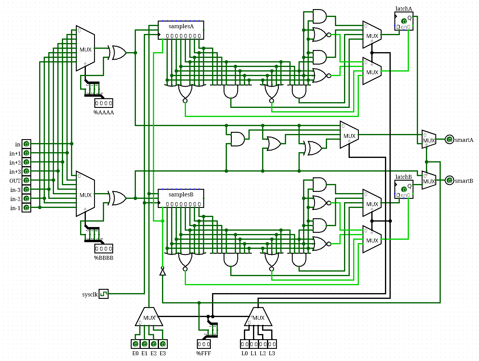
Here's a schematic I did of the F block which contains the A/B input selects as well as a de-glitcher for each. The exact logic is a guess of course.
EDIT: Typo correction - Mistakenly used majority in place of unanimous. Doh!
Thinking about an efficient bit-bashed SPI bus for the SD card I have come up instead with a routine that use the pulse mode for the clock and a frequency dependent delay before sampling 8 bits. I use 2 cycles high 2 cycle low with a delay before first sampling and then 8 pairs of testp and rcl. Clocking in 512 bytes of data takes 135us @200MHz.
This has resulted in a 3.5MB/s read speed using this technique and normally I would have to run the P2 at close to 340MHz to get this rate. I will test this out at different frequencies but it looks like I can clock it at its max of 50MHz with the P2 running at 200MHz using a very simple smartpin assisted bit-bashing.
I really need a 200MHz or better scope to see it better though, the clock is just a wavy line at present.
*** SPEEDS *** LATENCY......................... 489us,278us,258us,312us,279us,257us,313us,280us, SECTOR.......................... 371us,415us,394us,394us,413us,393us,394us,413us, BLOCKS.......................... 3,509kB/s @200MHzYep, that's exactly it Peter. The faster you push the SPI clock, the more you have to deal with fine tuning the lag compensation. In the end it's just an empirically found magic number.
You can do the transmit phase alignment testing, between clock and data, at a slower sysclock. Conveniently, as the SPI master, those stay aligned, albeit scaled by the sysclock period. I've often used 2 MHz sysclock for this.
Then only have to do the guessing of receive phase alignment testing (turnaround lag) at full speed. All delay components play into this, including the peripheral chip and circuit board characteristics. Which can mean a calibration round at driver init to handle different boards.
Actually I need a faster scope to check for wave shape and ringing, but this is all I can see with the 100MHz Rigol when I push it to a 60MHz SPI clock.
Is that cyan trace the data?
Yes, and that is the scope trying to render the $56 data as best as it can as both the analog bandwidth and the sampling rate are pushed.
There's something wrong there then. The clock is doing at least two transitions per data transition, it should be the most attenuated.
Is the probe switched to x1 maybe? That would kill the signal.
No, this is just the scope struggling to render an irregular signal. I checked it against a 50MHz Tek scope and it looked very similar too where it seems to have nice smooth waveforms for regular clock signals but the data always looks wonky. I'm looking at getting a better scope just so I can examine this signal better. Maybe somebody already has a good scope and can try this out?
The difference too is that the clock is from the P2 with a strong drive whereas the data is from the SD. I might try a CMD6 to enable high-speed drive.
The data is effectively a 30 MHz signal. It should be far more discernable than that on a 100 MHz rated front end. I'd expect a 20 MHz frontend to beat what you've got there.
Ah! Now we're talking. I thought it was tx from prop2.
You know the scope will severely impact the timing of rx. Don't expect any valid receive data while the probe is attached.
On the other hand, attaching a probe to tx will be fine timing wise.
Yes, I have been very familiar with all kinds of scopes for 50 years now. Even back in the mid 80's I had very expensive $25,0000 (in 80's $) HP MSOs that I used, and also good and trusty 4ch analog scopes at the time. If I am really interested in this signal I need to increase the drive, perhaps though a cmd6 or buffering, but I really want to see the higher frequency ringing components too.
I was just a bit surprised you were even looking at the rx data with the scope is all. Ringing won't be any worse at the higher data rate than it was before.
We are used to the limits and the effects of our test equipment on whatever we are testing. Increasing the clock does affect the response since the card controller is consuming more power and ground bounce and spikes are expected too.

Probes also start to go faulty so I swapped the data probe but also inserted a 100 ohm in series as well.
Still pretty much the same with this one at 80MHz.
I suspect the scope is showing you a reasonable representation of what's happening. And so there's no valid data coming back when the probes are removed.
What options is there for drive strength of the peripheral device?
I once tried the softkeys of the quickstart boards and realized that an open input "measures" the electrical field of the 50 Hz mains, so measuring the signal with the scope was impossible. I then realized: I do not want to see the signal but what the input sees. So I just used another cog to route the input to a free output and could measure the input signal from the sight of the input pin. Maybe that helps here too.
In the Spin2 doc, there is an example of capturing 330 MHZ pin activity via the streamer and then showing it on a DEBUG logic analyzer display. It's just a few lines of code to get the streamer to capture pin data.
(Oops, I drafted this way before in response to evanh and ErNa but didn't send it).
I know what the input sees because I am using TAQOZ to show me. I could use a logic analyzer instead and capture those signals but they will only tell me what I already know. Being fully aware of probe loading and even how a DSO physically and effectively samples and display a signal, I use all the imperfect tools I have, taking their limitations into account. So I'm not surprised at the data signal lumpiness because I'm also not surprised that the sine wave looking clock signal is somehow peaking at 4V and even going negative. But what I see and don't see tell me enough for the moment.
The data trace doesn't look right to me at all. You should be seeing rounded bumps that look the same as a single clock cycle. What does the tx data out of the prop2 look like?
Is it using Equivalent Time Sampling?
https://www.tek.com/document/application-note/real-time-versus-equivalent-time-sampling
https://www.ebay.com/itm/324361188151 - 250MHz bandwidth, 100MHz sampling, 25GHz Equivalent Time sampling, used usd375
If it is EQTime, you might want to try triggering on your data line.
That'll be the same as the repetitive mode I used on my old scope for the first time not so long ago - https://forums.parallax.com/discussion/comment/1478442/#Comment_1478442
The low-end Rigol's, at least, certainly don't have that.