

Accessing SD cards over 4 bit MMC bus
 Wuerfel_21
Posts: 4,463
Wuerfel_21
Posts: 4,463
Has anyone done it yet?
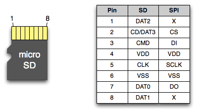
Annoyingly, the bootloader SD pins are arranged in a very unhelpful order for MMC bus (assuming we connect DAT1 and DAT2 to P56 and P57). Luckily, I think smartpins and the MERGEW op can make it work, anyways. Assuming 250MHz P2 clock, there's 5 cycles available per high-speed SD clock (50 MHz). There's no way to read 4 arbitrary pins and add them to a long in that time. But if we read 8 bits at a time with smartpins, we have 40 cycles to read the 4 smartpins and arrange the received data in a sensible way. I'm thinking this'd work (or something very similar, anyways)
'' The 4 data pins must be in 8 bit synchronous receive mode
'' SE1 must be set to the rising edge of any of them
'' Also need to somehow generate the clock pulses.
        rep @.rdlp,#128
        waitse1
        rdpin tmp,pin_dat3
        rolbyte lbuf,tmp,#3
        rdpin tmp,pin_dat2
        rolbyte lbuf,tmp,#3
        rdpin tmp,pin_dat1
        rolbyte lbuf,tmp,#3
        rdpin tmp,pin_dat0
        rolbyte lbuf,tmp,#3
        mergeb lbuf
        wflong lbuf
.rdlp
Perfect.
The next problem is generating the 50 MHz clock. Transitions mode would be ideal, but that can only do even periods, so it can only generate 50 MHz when sysclock = 50MHz*2*N. Most SD cards these days support UHS-1 modes though, so I'd assume they will accept slightly more than 50 MHz in normal modes? Would have to be tested. Not sure if 62.5 MHz is OK (250 MHz / (2*2)). The next step down would be 41.6 MHz. Still much faster than anything in SPI mode.
Also, the CMD pin needs to be handled somehow. I don't think there's anything happening on that line during transfers unless the host sends a command first, so fine I guess?
Another thing: What is CS in SPI mode becomes DAT3, so what about that flash that hangs off that pin? I guess it can be disabled using the DIP switches... OTOH, what's the point of using the boot SD pins when you're going to boot from flash? So it's fine I guess?
Comments
I could be wrong, but I don't think uSD will work in 4-bit MMC mode. Think it has to be SD mode.
And then, people have some reservations about using SD modes where there are some licensing issues...
But, if you need speed, I've gotten 8-bit MMC mode working with an eMMC chip.
SD bus == MMC bus, it's more or less the same thing.
I am fairly certain that licensing thing is a bit of a myth, but I couldn't care less either way.
Not yet to my knowledge no, but someone should. You'd have to rework the P2-EVAL for this to work however, so it is probably not something that will be widely usable by people at this stage. Ideally you fit an SD card to other pins to the flash but then you might need two SD cards if you are booting as well.
Your merge approach is pretty clever but I think it will prevent you from using the streamer as the COG will be busy doing the rearranging work (though some cycles are free in this loop which may help control the CMD pin).
If (as I suspect) you find you do have to stream to/from the pins you could wire the 4 SD data pins to the P2 in sequential pin order (so it sees DAT0-DAT3 as a full nibble aligned on an 8 bit P2 pin boundary such the pin streamer can be used) so no need to rearrange bits. You can probably still share the boot SD device if you just wire another 4 P2 pins to DAT0-3, duplicating the CS and DAT0 wiring again to other P2 pins. This risks shorting two P2 pins with errant software driving both these pins to different values but fixes the nibble issue, though a series pass resistor will help reduce that problem (the resistors are a good idea anyway for high speed operation to help signal integrity etc).
You can control the CMD pin independently with a smartpin to shift it serially for the commands and responses which can be managed in parallel to data transfers the streamer is doing, at times overlap required such as when cancelling multiple block reads. Serial or clocked smartpin mode should help this.
Getting the timing right will of course be critical between the end of the command and reading back data and you'll need to get it down to the precise number of clocks. This is probably why you'll need independent control and have the streaming happening in the background freeing COG cycles for this.
I think the flash will very likely drive its data pin output once you chip select it and it randomly receives a valid read sequence on its MOSI pin, so it could be a problem.... you might need to disable the flash to have this scheme work on the P2-EVAL. Easier to operate the two devices on different pins, but I know what you are hoping for.
I just planned on soldering an SD breakout board to one of those blank accessory boards. I think that's reasonable. Plugging it into the last socket only gives two unused pins though, so no way to arrange them ideally.
I guess it'd be better to ditch the built-in SD loader and just write a 4-bit one onto the flash.
Yeah good call. I still don't trust the SD+flash pin sharing scheme when you want to have both devices accessible at any time by any COG. I know it can probably be done in some usable way if COGs are coded to follow specific sequences and use particular SD cards etc, but it's a bit of mucking about to perfect. IMO it will be safer for P2 field deployments to just boot off flash, (Cluso may disagree, he likes SD ).
).
@Wuerfel_21
I haven't tried SD nibble access. AFAIK the commands are still issued as single bit wide commands.
For reading a whole sector, unless you can read two (2) sets of four (4) bits with clocking and packing up into a byte in less than 32 instructions then there is little point. My driver reads a byte as unravelled 8 bits (4 instructions per bit) and the whole 512 sector bytes are done in a zero cost overhead REP loop, and the crc (which is discarded) is read in 2 instructions per bit with crc being 16 bits. My code runs in cog/lut so the only hub access is to write out / read in the sector bytes. I haven't included this in the instruction count, but I'm using rfbyte and wfbyte so there is no hub slot delays as they are buffered.
Yes the commands are still single bit wide.
I believe that the streamer from 4 pins to the FIFO can do the data transfer for you with this sort of streamer command.
Just need to be careful to set the "a" bit correctly for the right nibble order in the bytes written into the FIFO then to HUB RAM. You can issue the streamer instruction (which only 2 clocks) and it will then read the given number of 4 bits into bytes and write these via the FIFO to the HUB RAM (don't enable DACs) in one go. You are sampling the 4 SD data bits at 50MHz so this is only 25MB/s worth of writes to the FIFO which should easily be able to keep up while still allowing plenty of memory bandwidth for other COG transfers in parallel.
If you use the streamer and if you want to check/build CRCs you'd need to have already generated this beforehand, or check after the data result is stored in HUB (which may slow things down slightly), though you might be able to rapidly transfer large 512 byte blocks into LUT with SETQ2 and do table based CRCs on them fairly quickly, or with CRCNIB etc...
The issue will be timing the input pins correctly to the output clock for the card in order to read the data at the precise time (but that can be done with care). Some input delays may also potentially need to be adjusted based on P2 clock speed (like HyperRAM does), due to the fixed latency of the P2 input path but the variable P2 clock period.