It always depends on which way you’re viewing it. That’s why they started using MOSI an MISO - master slave. But then you get two micros and who is the master?
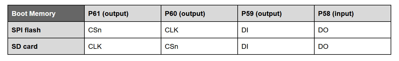
But that table is quite specific and correct. P59 is the output and DI on the flash/sd. BTW it can be O/I on a 3 wire SPI where the DO from SPI is wired to DI but you can ignore that here.
Yeah, it's labelled according to nominal wire/signal naming convention, ie: A wire/signal is named the same all the way through its path. In this case, the slave device has names for those signals and the Prop2 pins have no specific names other than P0,P1,P2 ... so Chip has adopted the the slave's naming for the Prop2 documentation.
The table is correct since I look at the Flash row and see that DI of the Flash is connected to P59. Perhaps more correctly the top row should have been labeled P2 in the left column, the same as "SPI flash" and "SD cad" and then the whole table labeled "Boot Memory connections" a header.
On my schematic though, I might label that signal (not the pin) as MOSI. Both are correct.
Thanks for clarifying that. This is what led to my initial confusion. My SPIN2 template always causes me to pause. Not sure why but I always have to work through the directions.
jonnymac's template style is to include:
{ I } to indicate that the propeller pin is set/used as an input
{ O } to indicate that the propeller pin is set/used as an output
I've started to also do:
{ SP } to indicate that the properler pin is in smart pin mode.
I reworked the P2 standard pin definitions for my handler/formatter code. Here is a copy 2021-Feb-19: Updated to fix typos in comment for shared pins with SD (was SF)
con { P2 I/O pins }

  SER_RX        = 63        { I }           '\ SERIAL: Recv pin: P2 programming / debug port
  SER_TX        = 62        { O }           '/         Xmit pin: P2 programming / debug port

  SF_CS         = 61        { O }           '\ FLASH:  Chip Enable pin    (shared with SD_SCK)
  SF_SCK        = 60        { O }           '|         Clock pin          (shared with SD_CS)
  SF_SDI        = 59        { O }           '|         Data In  MOSI pin  (to   Flash)
  SF_SDO        = 58        { I }           '/         Data Out MISO pin  (from Flash)

  SD_SCK        = 61        { O }           '\ SDcard: Clock pin          (shared with SF_CS)
  SD_CS         = 60        { O }           '|         Chip Enable pin    (shared with SF_SCK)
  SD_SDI        = 59        { O }           '|         Data In  MOSI pin  (to   SD)
  SD_SDO        = 58        { I }           '/         Data Out MISO pin  (from SD)
@"Francis Bauer" I understood the purpose of the { O } { I } indicators. I like them. It's the symbol names which keep throwing me out of kilter. I like your { SP } indicator, BTW.
I'm reading the symbol, SF_SDO, as this is the symbol for the pin reading data coming in from the flash which should be pin 58.
SF_SDO = 59 { O } ????
I'm reading the symbol, SF_SDI as this is the symbol for the pin writing data to the flash which should be pin 59.
SF_SDI = 58 { I } ????
The way Cluso marked the SD SDO as SD_SDO makes sense because I know it is the SD's SDO pin on P58. Of course from the P2's POV it is really a MISO
So, when read in a verbose way the symbols make sense.
The Serial Flash Chip Select is SF_CS which is connected to the output P61
The Serial Flash Serial Clock is SF_SCK which is connected to the output P60
The Serial Flash Serial Data In is SF_SDI which is connected to the output P59
The Serial Flash Serial Data Out is SD_SDO which is connected to the input P58
@CJMJ said:
@Cluso99 Shouldn't shared with SF_SCK be SD_SCK and SF_CS be SD_CS?
  SF_CS         = 61        { O }           '\ FLASH:  Chip Enable pin    (shared with SF_SCK)
  SF_SCK        = 60        { O }           '|         Clock pin          (shared with SF_CS)
Aha! I see what you mean in the comments. I fixed the earlier post.
No! They have deliberately been swapped so both Flash an SD can share the same 4 pins.
When using SD the Flash CS will go up and down (it’s the SD CLK) but the Flash CLK will remain low (it’s the SD CS). The opposite happens when using the Flash. So they both co-exist.
Otherwise, we would have needed an extra pin or an external inverter to separate the CS signals to opposite polarity.
Thanks Lachlan. I totally missed that.
It will take a while for me to get that run thru the various demo programs because we don't have include in pnut, and I try where possible to limit what will not compile with pnut/PropTool.
Updated the above post with corrections.

 CJMJ
Posts: 225
CJMJ
Posts: 225

Comments
It always depends on which way you’re viewing it. That’s why they started using MOSI an MISO - master slave. But then you get two micros and who is the master?
But that table is quite specific and correct. P59 is the output and DI on the flash/sd. BTW it can be O/I on a 3 wire SPI where the DO from SPI is wired to DI but you can ignore that here.
Yeah, it's labelled according to nominal wire/signal naming convention, ie: A wire/signal is named the same all the way through its path. In this case, the slave device has names for those signals and the Prop2 pins have no specific names other than P0,P1,P2 ... so Chip has adopted the the slave's naming for the Prop2 documentation.
The table is correct since I look at the Flash row and see that DI of the Flash is connected to P59. Perhaps more correctly the top row should have been labeled P2 in the left column, the same as "SPI flash" and "SD cad" and then the whole table labeled "Boot Memory connections" a header.
On my schematic though, I might label that signal (not the pin) as MOSI. Both are correct.
I added input and output directions to the SD/Flash pins in that table.
Thanks for clarifying that. This is what led to my initial confusion. My SPIN2 template always causes me to pause. Not sure why but I always have to work through the directions.
Do you see my confusion or is it just me?
jonnymac's template style is to include:
{ I } to indicate that the propeller pin is set/used as an input
{ O } to indicate that the propeller pin is set/used as an output
I've started to also do:
{ SP } to indicate that the properler pin is in smart pin mode.
Does this help resolve your confusion?
I reworked the P2 standard pin definitions for my handler/formatter code. Here is a copy
2021-Feb-19: Updated to fix typos in comment for shared pins with SD (was SF)
con { P2 I/O pins } SER_RX = 63 { I } '\ SERIAL: Recv pin: P2 programming / debug port SER_TX = 62 { O } '/ Xmit pin: P2 programming / debug port SF_CS = 61 { O } '\ FLASH: Chip Enable pin (shared with SD_SCK) SF_SCK = 60 { O } '| Clock pin (shared with SD_CS) SF_SDI = 59 { O } '| Data In MOSI pin (to Flash) SF_SDO = 58 { I } '/ Data Out MISO pin (from Flash) SD_SCK = 61 { O } '\ SDcard: Clock pin (shared with SF_CS) SD_CS = 60 { O } '| Chip Enable pin (shared with SF_SCK) SD_SDI = 59 { O } '| Data In MOSI pin (to SD) SD_SDO = 58 { I } '/ Data Out MISO pin (from SD)@"Francis Bauer" I understood the purpose of the { O } { I } indicators. I like them. It's the symbol names which keep throwing me out of kilter. I like your { SP } indicator, BTW.
I'm reading the symbol, SF_SDO, as this is the symbol for the pin reading data coming in from the flash which should be pin 58.
SF_SDO = 59 { O } ????
I'm reading the symbol, SF_SDI as this is the symbol for the pin writing data to the flash which should be pin 59.
SF_SDI = 58 { I } ????
The way Cluso marked the SD SDO as SD_SDO makes sense because I know it is the SD's SDO pin on P58. Of course from the P2's POV it is really a MISO")
So, when read in a verbose way the symbols make sense.
The Serial Flash Chip Select is SF_CS which is connected to the output P61
The Serial Flash Serial Clock is SF_SCK which is connected to the output P60
The Serial Flash Serial Data In is SF_SDI which is connected to the output P59
The Serial Flash Serial Data Out is SD_SDO which is connected to the input P58
@"Peter Jakacki" Yes! That's the way my brain is interpreting it. Thanks.
@Cluso99 Love it! Thanks for the snippet.
@Cluso99 Shouldn't shared with SF_SCK be SD_SCK and SF_CS be SD_CS?
  SF_CS         = 61        { O }           '\ FLASH:  Chip Enable pin    (shared with SF_SCK)
  SF_SCK        = 60        { O }           '|         Clock pin          (shared with SF_CS)
Aha! I see what you mean in the comments. I fixed the earlier post.
No! They have deliberately been swapped so both Flash an SD can share the same 4 pins.
When using SD the Flash CS will go up and down (it’s the SD CLK) but the Flash CLK will remain low (it’s the SD CS). The opposite happens when using the Flash. So they both co-exist.
Otherwise, we would have needed an extra pin or an external inverter to separate the CS signals to opposite polarity.
Its just the comment that needs changing, those F's need to change to D's just on those first two lines Ray. I noticed it too, but its pretty minor
Thanks Lachlan. I totally missed that.
It will take a while for me to get that run thru the various demo programs because we don't have include in pnut, and I try where possible to limit what will not compile with pnut/PropTool.
Updated the above post with corrections.