

Can you give comments on my PCB layout? :)
 Mohamed_Faris
Posts: 5
Mohamed_Faris
Posts: 5
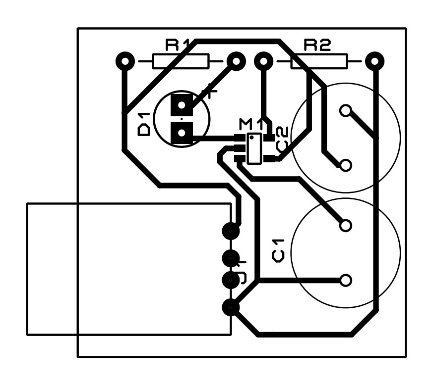
Hi, I am new to PCB design, so could you please give some comments on my first PCB layout? The circuit is for a charging controller using MCP73831 IC.
Note that the part getting out of boundaries is for a USB port, so it can have a small part out of the chip. You can give comment on anything nevertheless!
I tried to follow the best practices for a PCB to be manufactured (No specific manufacturer) .
Thanks in advance ![]()
Comments
Your layout is workable, but I would consider the following changes that would reduce traces lengths:
In my PCB experiences, shorter straighter traces are desirable.
I would include a ground plane on the PCB. I assuming C1, C2 are electrolytic capacitors, if so please add the appropriate '+' symbols.
I didn't verify that the layout is accurate electrically, hopefully it is...
Keep up the good work.
Get rid of those T intersections!
Connect J1 to C1 and from there to M1 and C2, then from C2 to R2. Then M1 directly to C2, then to R1.
And I agree about the ground plane.
-Phil
That layout doesn't make any sense, the only connection I can see is to the ground and VBUS of the USB connector, and why would you ever need huge ecaps? If it is a charger then it must handle current and this should also be reflected in the tracks which look like they would burn out or drop too much voltage with too much current etc.
A PCB layout must have a schematic which you would always post with any pcb layout you are seeking critique for
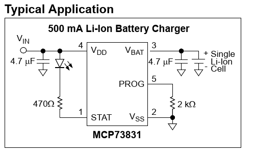
EDIT - I looked at that chip and it only needs tiny caps (even ceramics about the same size as the chip) - but still you need a connector for the battery it is intended to charge.
Thank you all for your comments.
Hi Phil, I understood your recommendations, however, I have read read before that Daisy chain is not preferred with power rails, so I thought that is preferred with ground as well.
Hi Peter, you are right, I should have put the schematic. For the tracks, they are much wider than the width required for a 1 Ampere current, given that the battery is 90 mAh. Regarding the ecabs, I just wanted to use all components to be through-hole components as I read that they are more reliable.
I gave explanation of what I did to understand more from you, and again thanks a lot.
attached is the schematic, and the package used.
At the very least, then, straighten out those acute junctions, and add some fillets where the traces join. But, since you're saying that's a ground trace, use a ground plane on the other side of the board instead.
-Phil
Understood, thanks a lot for the help.
Since "ground plane" has been mentioned ... don't confuse this will a "flood fill".
Typically when I lay a board out:
Thanks Baeu a lot for clearing these things out. Really, appreciate your instructions.
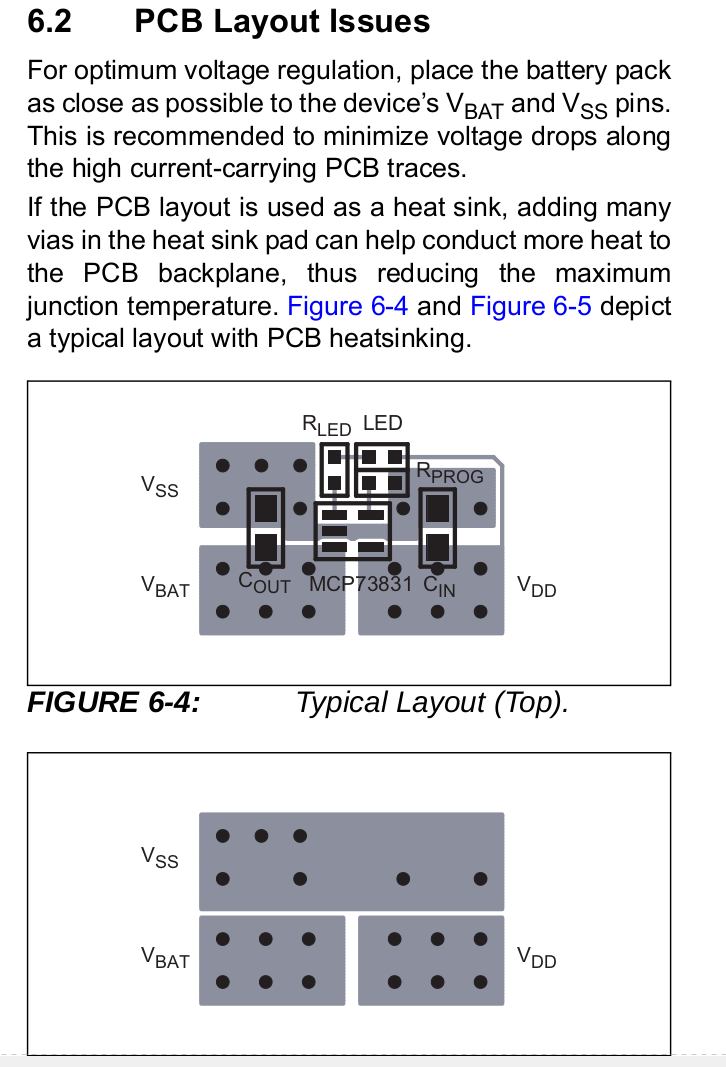
Sure, you can cobble a pcb together and it will "work" even though you have to solder directly to the huge capacitor pins poking through the bottom because all your tracks are on the top side itself and you haven't allowed for the battery connection. Then you will have to drill out the pcb for the lugs on the USB plug or allow for some mechanical support since it will undergo stresses. But the huge caps indicate that you do not know how big a 4.7uF capacitor is at all and what type is best etc. Having " read that [through-hole components] are more reliable" is what you have read somewhere, but is not a fact. But 4.7uf ecaps would be the same size and have the same footprint as the LED (which btw should have some kind of polarization marking or a square pad etc). Your footprint could take a 4,700uF ecap but 1,000 times more is not 1,000 times better. Above all, RTM (Read The Manual), especially "6.1.1.3 Thermal Considerations" but here's the section talking about the caps.
BTW, none of us would ever lay out this simple circuit this way, and the board would be way smaller too and less likely to break the plug etc.
Think about how the pcb plugs into the USB port and what will be in the way with your pcb sticking out so wide. Make it slender like a Flash drive instead.
Finally - what the manufacturer says about pcb layout itself. (note the so called "less reliable" smd caps too)
Thanks a lot for the feedback. You made things clear.
For through hole components soldered to the ground plane or any large copper area, consider adding thermal relief to make soldering or rework easier and more reliable. Can't tell you how much linguistic peeling of paint occurs when the solder just can't seem to melt right.