

Faster communications between cogs???
 Cluso99
Posts: 18,069
Cluso99
Posts: 18,069
in Propeller 2
On numerous occasions I have not been able to achieve something on the P1 because I could not get data between cogs quick enough.
Others, including myself, have said it was a shame the Port B had not been implemented internally so we could use these 32-bits to communicate between cogs.
In the P2Hot we had a bus between cogs plus instructions to assist. But this is not in the P2.
I have been playing with USB LS again in the P1. There are all sorts of tricks to read the USB LS bus. Let me explain where I am up to..
Each USB LS bit comes in at precisely every 64 clocks when overclocking P1 to 96MHz. This means 16 instructions for most instructions. Here is a sample piece of code for a LS bit time...
Now, if you unravel 8 bits, then there are 4 usable nop instructions (16 clocks) in which to process the received bit. So there is time to use waitcnt (7+ clocks) with a jmp/djnz (4 clocks to loop, 8 clocks if jump not taken).
However, once 8 bits have been assembled, you must pass this character to another cog for processing, while the code goes back to get the next character.
This is where the problem arises as there are only 4 instructions or 16 clocks in which to write the byte to a hub buffer. To write to hub takes from 8-16 clocks. BUT we don't know where the hub is up to, so the hub write is INDETERMINATE. We don't have the time to use a WAITCNT to resynchronise either.
To get around this problem I stole 10 I/O pins to pass the data byte to the assisting cog. 8 bits are for the data byte, 1 bit is used if the byte is a control character (SYN/EOP/etc), and the last bit is used to signal a byte is available. Of course this is unsatisfactory in a production environment because there aren't normally 10 spare I/O on a P1 circuit.
P2
Chip has implemented the USB serial in the smart pins which will improve timing dramatically. USB is a special case.
The P2 instructions will be 2x faster, the clock will be 2x faster (160+MHz) so that makes it basically 4x faster than the P1. But USB FS is 8x faster than USB LS (12MHz vs 1.5MHz). And then we are overclocking the P1. Will the P2 achieve 192MHz ??? If so, then without the smart pins we are >2x slower to do USB FS 12MHz.
Where am I going with this?
Well, the P2 has lots of cogs to do processing I/O. Smart Pins will help in many, but not all, situations. The cogs are only half the speed of the P2Hot (an accepted reality).
How can we get cogs to co-operate better without overcomplicating the current design? <ducks for cover>
Suggestion
Might it be possible to place a unidirectional latch between each adjacent cog? <ducks for more cover>
Here is the idea..
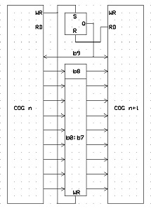
Each cog has a 9 bit internal output latch joined to the next adjacent cog as an input latch. An additional latch bit is set when the latch is written by the cog, and is cleared when the adjacent cog+1 reads the latched 9bit data.
Additional instructions required...
WRCOG D/# [WC,WZ]
Writes the 9 bit D/# data to the latch (to COG+1) and sets the DataAvailable latch (depends on WC/WZ setting below).
If WC is specified, then if the DataAvailable latch is already set (ie the next cog has not read the data) then the data will NOT be written and the C flag will be set.
If WZ is specified, then bit8 of the latch will be masked OFF, irrespective of bit8 in D/#.
RDCOG D [WC,WZ]
Reads the 9 bit data from the latch (from COG-1) and clears the DataAvailable latch (depends on WC/WZ setting below)
If WC is specified, C will be set if the DataAvailable latch was previously set (ie data is valid).
If WZ is specified, then bit8 of the latch read will be masked OFF, and Z will be set to the original bit8 value.
Dare I ask if this is possible and easy to do???
Others, including myself, have said it was a shame the Port B had not been implemented internally so we could use these 32-bits to communicate between cogs.
In the P2Hot we had a bus between cogs plus instructions to assist. But this is not in the P2.
I have been playing with USB LS again in the P1. There are all sorts of tricks to read the USB LS bus. Let me explain where I am up to..
Each USB LS bit comes in at precisely every 64 clocks when overclocking P1 to 96MHz. This means 16 instructions for most instructions. Here is a sample piece of code for a LS bit time...
rxbit         test      state_k, ina   wz       '4 04   z=J/SE0 nz=K/SE1        | nc | SE0 | SE1 |
              test      state_jk,ina   wc       '4 08   c=J/K   nc=SE0/SE1      | c  |  J  |  K  |
        if_nc jmp       #SE0_SE1                '4 12   j if SE0(EOP)/SE1(error)
              muxz      prev, bit30    wc       '4 16   c=!current bit (prev^current) (c=1=clock="0"bit)
              shl       prev, #1                '4 20   shift current J/K into previous J/K
              rcr       data, #1                '4 24   collect inverse data bit (lsb first)
              test      crc, #1        wz       '4 28   z=crc[0] & c=!current; now accum crc..
 if_nc_and_z  xor       crc, poly               '4 32   if  !curr=1 & crc[0]=0 then crc=crc^poly     ????
 if_c_and_nz  xor       crc, poly               '4 36   +if !curr=0 & crc[0]=1 then crc=crc^poly     ????
              shr       crc, #1                 '4 40   crc>>1
              rcr       stuffcount, #6 wz       '4 44   z=(6x1's) so unstuff next
        if_z  call      #rxunstuff              '4 48   unstuff next bit
              nop                               '4 52
              nop                               '4 56
              nop                               '4 60
              nop                               '4 64
Now, if you unravel 8 bits, then there are 4 usable nop instructions (16 clocks) in which to process the received bit. So there is time to use waitcnt (7+ clocks) with a jmp/djnz (4 clocks to loop, 8 clocks if jump not taken).
However, once 8 bits have been assembled, you must pass this character to another cog for processing, while the code goes back to get the next character.
This is where the problem arises as there are only 4 instructions or 16 clocks in which to write the byte to a hub buffer. To write to hub takes from 8-16 clocks. BUT we don't know where the hub is up to, so the hub write is INDETERMINATE. We don't have the time to use a WAITCNT to resynchronise either.
To get around this problem I stole 10 I/O pins to pass the data byte to the assisting cog. 8 bits are for the data byte, 1 bit is used if the byte is a control character (SYN/EOP/etc), and the last bit is used to signal a byte is available. Of course this is unsatisfactory in a production environment because there aren't normally 10 spare I/O on a P1 circuit.
P2
Chip has implemented the USB serial in the smart pins which will improve timing dramatically. USB is a special case.
The P2 instructions will be 2x faster, the clock will be 2x faster (160+MHz) so that makes it basically 4x faster than the P1. But USB FS is 8x faster than USB LS (12MHz vs 1.5MHz). And then we are overclocking the P1. Will the P2 achieve 192MHz ??? If so, then without the smart pins we are >2x slower to do USB FS 12MHz.
Where am I going with this?
Well, the P2 has lots of cogs to do processing I/O. Smart Pins will help in many, but not all, situations. The cogs are only half the speed of the P2Hot (an accepted reality).
How can we get cogs to co-operate better without overcomplicating the current design? <ducks for cover>
Suggestion
Might it be possible to place a unidirectional latch between each adjacent cog? <ducks for more cover>
Here is the idea..
Each cog has a 9 bit internal output latch joined to the next adjacent cog as an input latch. An additional latch bit is set when the latch is written by the cog, and is cleared when the adjacent cog+1 reads the latched 9bit data.
Additional instructions required...
WRCOG D/# [WC,WZ]
Writes the 9 bit D/# data to the latch (to COG+1) and sets the DataAvailable latch (depends on WC/WZ setting below).
If WC is specified, then if the DataAvailable latch is already set (ie the next cog has not read the data) then the data will NOT be written and the C flag will be set.
If WZ is specified, then bit8 of the latch will be masked OFF, irrespective of bit8 in D/#.
RDCOG D [WC,WZ]
Reads the 9 bit data from the latch (from COG-1) and clears the DataAvailable latch (depends on WC/WZ setting below)
If WC is specified, C will be set if the DataAvailable latch was previously set (ie data is valid).
If WZ is specified, then bit8 of the latch read will be masked OFF, and Z will be set to the original bit8 value.
Dare I ask if this is possible and easy to do???
Comments
That's true the first time around, but the SysCLK is 6 x 16, which gives you a special case, I think ?
ie you will slew a little, to phase sync, but then continue correctly ? 1/6 is probably just tolerable ?
Mail box type access has merit, but that is one way only, and a down side is you start to lock COG placements.
Some small Dual port memory (naturally 2 way) in LUT space may be better ?
This would place the COGS in a ring, so every COG can talk left and right.
But I did not want to create anything complex. Just an easy method that doesn't take much silicon and little work.
Have you considered that you can set up 64n-byte rings in hub RAM that you can write in 2 clocks from one cog and read in two clocks from another cog? There is a problem with knowing WHEN a new byte was written, which could require a strobe of some kind between cogs.
I will look at the 64-n byte rings you mention below.
No. Is there a writeup anywhere? I don't recall seeing that info although I do recall having a small block that could be written in hub that triggers an interrupt to another cog. Is this what you are referring to?
I'm just talking about setting up a loop in hub RAM using WRFAST in one cog and RDFAST in the other, so that WFBYTE/WFWORD/WFLONG instructions could write and RFBYTE/RFWORD/RFLONG instructions could read a loop of memory.
What is the shortest latency possible with WRFAST and RDFAST, assuming ideal phase-align.
ie should COG+1 or COG+2 or COG+3 be the nearest-in-flight-time target ?
Given the eggbeater gives a naturally fast-direction, should any simpler mail-box ports 'face the other way', to complement that ?
If you have enough capacity in the COGRAM you might be able to do a table lookup for a CRC16 on your P1 too. Remember once you go to a byte based CRC you are only needing to do the CRC operation once per byte, instead of using 4 instructions per bit for accumulating a CRC. So for 7 of the 8 USB bits you can then save 4 instructions. This may buy you enough time to do both the hub RAM write and the WAITCNT to resync (worst case is 22 + 5 clocks I think) just once after per 8 bits. Some 7 instruction slots are required for these 27 clocks. You seem to have 4 free plus the 4 saved per bit, which may just make it.
In fact I am thinking to save COGRAM space you may even be able to do the CRC16 table lookup using the table in HUB RAM too, with the workload evenly distributed over the available NOP instructions remaining in the other 7 received USB bits. It may be lagging by one byte but that may not matter too much.
What has not been shown is crc generation may be crc5 or crc16, depending on the token type.
Lookups just shift the problem from one area to another. If the table is in hub, then the same problem arises. How do you interleave the lookup within the reading of bits? The timing is indeterminate. Even using unravelled code, one has to be careful that you can jump out of the unravelled code at various points.
Also remember that each block of data is not directly synchronised, so using waitcnt after a wrxxxx is required to keep in sync. As an addition to this, we don't want to shift sampling far from the centre of the bit as our clock is not synchronised to the USB clock, and over a large block there will be some clock slippage either way.
If you use the example of USB as I have done, then if the lookup is in hub, you have to hold over the crc calculation until the end of the received block. But this is where we are even more pressed for time due to the turn-around time required. If we calculate the crc along the way, then we only have to check the result is zero at the end of the block.
The WFBYTE/WORD/LONG might be a good way to pass data between cogs via hub, but it is certainly not as efficient as passing directly between adjacent cogs.
A WFxxxx will take 2??? clocks to setup, plus 1-16 clocks to wait until the hub address comes around. Then the receive cog will need to test/read the byte/word/long. This will take 2??? clocks to setup, plus 1-16 clocks for the hub address to come around, this being determinate on the cog number plus the hub address (least significant nibble).
Buffered writes don't have this issue. The Prop2 has optional buffered writes using WFxxxx instructions. No stalls need occur.
There was discussion for making all Hub writes buffered but Chip got busy on more pressing issues I think - http://forums.parallax.com/discussion/comment/1353203/#Comment_1353203
Instruction stalling is what you are really trying to avoid, not data lag. With high throughput and no stalls at your disposal, the Prop2 Hub is already pretty damn cool.
Just issue a WRFAST instruction and you have 2 cycle hub ram writes.
Now, I suppose that this would be no faster than Cog N writing the lazy-susan hub just before Cog N+1 got access to the same slice of memory, but I think it would be, on average, 8X faster for any two abitrary cogs seeking to communicate, and would do so in a fixed time. It wouldn't be faster than sharing via the pins, of course, but that would likely hog pins.
Perhaps this could be useful for sharing video data among multiple helper cogs for overlays or something like that (though I don't exactly have a specific use-case in mind with advantages), or maybe it could allow one cog to monitor the state of another cog or set of cogs. For example, a monitor cog could get the shared state of any other cog by performing a "tunnel destreg, sharedcognum" or similar. Anyway, it just "feels" like it could be useful for something if not a lot of "somethings," and the lack of such functionality *might* be seen as a lost opportunity or even a glaring omission (though probably not). So I guess that should be taken into consideration when evaluating the logic expense (and seeing if the timing would work out and so on).
If their critical loop is 16N cycles, later delays are less.
I think there may be an ideal landing COG-distance, with the eggbeater, for least latency streaming.
It may be some small number of sysclks later that the receiver can read, so that relative spacing could be chosen.
It's a little more work, but anyone chasing individual SysCLKs is well used to a little more work
The point is that to be cycle-paranoid (as you put it) requires knowledge of
1. Hub address (least significant nibble)
2. Cog number
3. Clock cycle that the asynchronous block transfer begins (every block varies!!!)
By the time all these are known, there is insufficient time to rearrange the instruction mix in the correct order to achieve the precise order required to be in phase. Under the timing constraints I am using, it is not possible to compile on the fly.
I don't mind a little more work, nor a lot more work. I am used to doing this on the prop - you should see some of my programs for proof.
But this is close to being impossible.
Agreed I am pushing the envelope here, but if a solution is both easy to implement and uses little silicon, then I am all for it. I am sure there are numerous cases where the P2 can be used to monitor/interface to other fast communications where the smart pins cannot do the job alone. I am just presenting a current case where I am trying to implement USB FS prior to having FPGA code.
2) Yes, but you know and define that
3) Yes, but that is Eggbeater determined
I can see that first-phase is more variable than repeated-phase, unless additional work is done.
How does P2 USB hardware manage Clock extraction, aka edge re-sync.
Does it resync the NCO on USB edges ?
HubRAM write buffering is the solution.
Getting it implemented for all Hub write instructions, rather than just the WFxxxx instructions, would be the next improvement.
I was opting for a simpler approach that also had less lag between cogs.
2) May not be known at compile time. A restriction to any pair of cogs is easier than restricting to a single cog of 16.
3) NO NO NO. Its both a mix of the egg-beater plus the clock skew of the first "K" transmission of EACH BLOCK. Every block will be DIFFERENT!!!
First of all, consider these two lines: They can be simplified to one instruction: That gets you 20 free clocks. That's enough for an "add ptr, #1" and a reasonably well aligned (i.e. 16 clock max) WRBYTE, which in your case is possible. The timing can easily be made determinate if you do it right. It's not indeterminate at all. Hub cycles come every 16 clocks and take 7 clocks at optimal timing. I'm not sure how many of the 7 clocks are before or after synchronization, but it doesn't really matter once you're synchronized. Once you've synchronized with the hub once, as long as you only do 4 or 8 clock instructions and as long as you make sure that (number of 4-clock instructions between hub operations) mod 4 == 2, every hub operation will take exactly 8 clocks. They will take 8 and not 7 clocks because, with that alignment, you will always get there exactly one clock early and will have to wait a clock. I'm pretty sure any (but not more than 4) nops immediately before the hub operation can be removed - they should just cause the hub operation to block for 4 more clocks.
At the higher level of use, using HubRAM as an effective DMA buffer has huge timing benefits for software. The need for tight Cog synchronisation melts away in nearly all cases. And, of course, the HubRAM based buffers can bridge between any Cog to any Cog or Cogs.
P2 will be dealing with bytes, rather than J and K transitions that will be managed by the smart pins. However I think Cluso is just using USB as an example to questions how cogs might co-operate for pipelining applications (usb, filters, dsp etc).
I think the answer is not to dwell on individual hub addresses until the last stage of writing final data to hub. As chip says you have a 64n bytes of hub buffer. The leading cog waits for the K edge (or whatever), then writes its
result to hub, which might go anywhere within that 64n byte (16n long) block. No matter where it goes, there's a cog that can pick that data up on the next cycle, process it, and write it back to hub in a same or different 64n block. All this is locked together, but it doesn't matter which phase the K edge starts on, the pipeline will do its job. By the time the final data is written, its likely to be at lower bandwidth due to the intermediate processing by the other cogs.
This dedicated write FIFO makes use of, as does a single write buffer, the Hub's fully random access SRAM speed that has been missing, a bit like an Achilles Heel, for the Prop. All Cog instruction writes become regular two clock instructions. That's pretty powerful.
Such a dedicated write FIFO would require a decent amount more flops compared to just a single buffer but wouldn't be huge. Say four deep, and like a cache in it's selective addressing except it is still purely a FIFO in terms of being write only. This allows impressive enough sustained throughput to never want to use the existing WRFAST features, leaving the existing FIFO for all it's other usefulness, while at the same time opening up fast writes to fully random addressing!
There are special cases, which can be best handled by smart pins, but what happens when you have an acquisition problem that requires speed and doesn't lend itself to using a smart pin?
Typically, you can buffer the incoming data to be acted up by another cog... the speed at which you can buffer and signal the other cog, the size of the buffer you can live with, and the amount of processing required per acquisition establish the limits.
Anything that improves this general process is worth going after... particularly if as Chip says, it takes practically no logic.
The issue with rdfast and wrfast is that they use the same bus... I think;) This means that if you are writing at 2 clocks per byte... it is still going to take you many more clocks to read anything from the Hub using a standard rdbyte while you are also wrfast-ing to it. This delay is built in and there didn't seem to be an easy way around it... until Cluso made his suggestion.
With Cluso's change, you can hand off the data to be acted upon by a second cog almost concurrently and if the further processing takes about the same number of instructions as the initial detection and offloading, the buffer size could be almost nil.
Ken,
I find Omeprazole to be highly effective at times like these:)
Don't listen to the commercials; omeprazole tablets act almost instantly.
The capsules take longer and are harder to swallow.
I use the Equate brand. It is worth its weight in gold.
The exclusive nature of the FIFO is the original reason I'd been pushing Chip to have a simple write buffer. The existing FIFO has the capacity to handle sequential circular reads without stalling. Writes don't need such a deep FIFO to achieve the same.
Here is an example... which doesn't exactly make my point, but got me listening to Cluso.
I was trying to get my PropCam to behave itself. Phil's assembly is pretty straight forward, but he also throws away some bits.
The PropCam has a serial mode, where the eight bits start coming in after a one clock pulse on a sync line.
This had me stuck for a while, so I decided to just dump all of the incoming data to a hub buffer and then look at it.
My thinking was that we have 40MIPs available... we have a 10MHz signal coming in... we should have four instructions to do whatever it is that we want... 3 if we want to be on the safe side... 2 if we want to follow the actual rules.
the routine for doing this is my kind of simple:)
 wrfast #0,##_Off_Screen_Buffer
            wrbyte #1,##1000002             'tell the analysis cog to start
            mov myreps,##500000
            rep @get_itall,myreps
            wfbyte ina
            'nop goes here for second test
get_itall
I don't have any labels on the pictures... the top line is the data bit line, the second line is the data sync and the bottom two lines are the high and low of the camera clock.
The first picture is without a nop. The second shows what happens to the clock by adding a nop... apparently the rules actually work:)
It's not the best example, because we only have room for one instruction... doesn't exactly scream out "Nobel Prize for Cluso,"
but its the idea that counts.
Some of you have made suggestions of how to change the code to get more free clocks.
Firstly, this code is for the P1 running at 96MHz. The P2 instructions will run 2x as P1. P2 will clock 2x P1 (ie 160MHz, NOT 192MHz which is 2x P1 when overclocked).
Secondly, the code is for LS, NOT FS which is 8x faster.
So the point is this...
If you want to sample a 12MHz signal (without Smart Pins which may not work for whatever case you are talking about), it is quite likely that a single cog will not do the trick. If that is the case, you might be in trouble passing 8-bit data to another cog to do further processing.
According to Chip, for a miniscule piece of silicon and time, an alternative to pass data bytes between adjacent cogs could be very effective.
Electrodude,
You are missing the point. Without the option of buffering with WFxxxx, it is necessary to add in a waitcnt (8 clocks minimum) plus a WRxxxx (8-16 clocks). But you have to allow for the whole 16 clocks for the WRxxxx plus the 8 clocks for the waitcnt. So that is 24 clocks of the 64 clocks available. Without these 24 clocks the timing is INDETERMINATE. And that is just to pass the data byte to hub. Then the other cog has to fetch it, once available.
Now the other solution proposed by jmg was to determine which cog you are (usually at runtime), determine where the buffer is in hub (lowest 6 bits are the relevant ones) (again usually at runtime). Now you wait for the first data bit of the block. Once this happens, you have to do the calculations to work out the best organisation of the WRxxxx instruction and the two adjacent instructions, and re-order them to suit the current hub slot with reference to the cog number, hub address, and the clock that the first data bit of this block commenced. You have to repeat this process for EVERY block of data. And you have to intertwine all of these calculations in between reading the bits, all while also handing bit unstuffing.
So, if you want to do NRZI and an alterntive protocol such as SDLC, the smart pins may not work for you. Here, IIRC DLE + SYNC is inserted every so often to ensure the receiver remains in sync with the transmitter.
There have been so many times that I could not do something because I couldn't get data between cogs fast enough. Some of these have been covered with streaming, the egg-beater hub, block read/writes, smart pins. But other cases still exist.
I was a big proponent of having an extra 32 bit I/O bus on the P2Hot (and earlier incarnation). But the sad reality is that this is a big ring around the outer part of the chip, and therefore consumes a lot of silicon vs benefits.
Yes. Every time the DP or DM line changes, it sets the NCO to halfway, so that it rolls over in half a bit period and on every bit period thereafter.