

P2 Reference Power Supply Circuit
 ke4pjw
Posts: 1,079
ke4pjw
Posts: 1,079
in Propeller 2
Is there a reference power supply circuits available for the P2? I am about to start a board layout for my retro computing project that uses a P2 and would like to go with a solid reference design.
Also, does anyone have a component already configured for the P2 ExpressPCB?
Thanks!
--Terry
Comments
The Edge board is a good one. It takes 5 volt input and splits that into a 1v8 switchmode for VDD and multiple 3v3 LDOs for the various VIOs. https://www.parallax.com/package/p2-edge-module-schematics/
The Eval board is similar but uses the USB 5 volts and USB controlled switches. https://www.parallax.com/package/propeller-2-evaluation-board-rev-c-schematics/
I use a dual SMPS MPM38222 chip with integrated magnetics for the 1.8V and another set for 3.6V which then feeds into a tiny dual 3.3V regulator. This makes for a very compact footprint while handling 2A for each supply with the 3.6V useful for external circuits. The 3.3V LDOs will only need to drop 300mV rather than the full 1.7V and so power dissipation and input current are reduced greatly.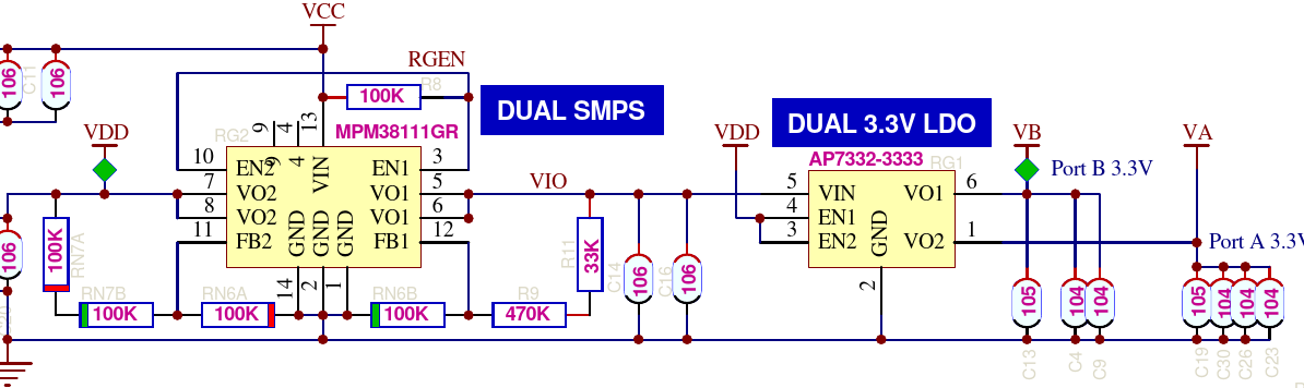
As a side note, I'd be interested in hearing more about your project...
My siolution takes a little more board space due to the external inductor and is a bit less efficient as Peters. But BOB cost is well below $1.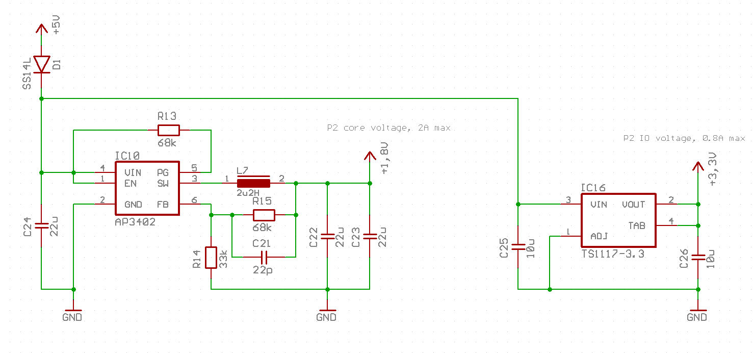
Schematic and PCB files (Eagle) are in the KISS board thread.
Thanks for all the responses!
Looking at the board, it appears you only power every other 1.8v pin, which I assume is for the core. Is that correct? Also, what size decoupling caps are appropriate? .1uF? (104)
This is my first layout that is all SMT, using new version of the software I know (ExpressPCB), first card edge connection I have had to design, and obviously, the first P2 board. I feel like I am stuck in the mud trying to get it done, LOL.
As always, thanks in advance.
Terry
All the 1v8's are connected via the square ringmain inside he pins. He's just decoupling every second 1v8 pin with a cap.
0.1uF caps are pretty light on for what can be up to 2 amps being consumed on that rail, i'd go for 1uF at least. It also depends on what regular you're intending to use, and what frequency you want to supress the most
Regarding regulators, we're using and happy with MEZD71202A-D, which works with 5v, 12v, or 24v input, and delivers 2 amps at 1v8. Its convenient to get started with because its in the same TO-220 form factor as 7805 series regulators
https://au.mouser.com/datasheet/2/277/mEZD71202A-1384003.pdf
Sokath, his eyes open!
I didn't see it before! So that ring is a trace that runs between the ground/heatsink and the pin pads. Got it! Not sure how I missed that!
Thanks!
Also, I see these are indeed .1uF (100 nF) decoupling caps.
You will also need some bulk capacitors spread around those pins too. 4u7F -10uF. And don’t forget X5R or X7R on all bypass and bulk caps - none of the Smile z5U etc.
The idea is to place many low-ESR caps as close as possible to the supply pins and at least one bigger cap somewhere else. Electromagnetic waves travel with ~2/3 of the speed of light on PCB traces. That's roughly 1m/5ns or 1"/125ps. So if the big bulk cap is 1" away the smaller caps have to provide enough charge to keep the voltage high enough. 8 x 0.1µF = 0.8µF discharged by 2A for a duration of 125ps would cause a voltage drop of 0.3mV. So the capacity of the smaller caps are not the problem.
But let's assume the switching regulator runs at 1MHz and needs 5µs to react to load changes. Then the bulk capacitor needs to be at least 100µF to keep the voltage drop below 50mV after a current change of 1A.
There have been lots of discussions about decoupling caps. Some say that you should also place an even smaller cap (say, 100pF 0402) with very low HF losses (C0G dielectric) in parallel to each 0.1µF cap. But I doubt that this has much advantage for P2 designs as the parasitic inductance of the bond wires and pins of the QPF-100 case is larger than the ESR of the capacitor.