

Bitbanging SPI driver timing problems
 ManAtWork
Posts: 2,076
ManAtWork
Posts: 2,076
in Propeller 2
Chip posted a nice example for using smart pins and the streamer for SPI data transfer in his boot loader. Unfortunatelly I can't use the streamer in my own code because I'd like to make it callable from fastspin code (HUB instruction fetch) instead of running in its own cog.
As my (cheap) flash chips only support 50MHz reads and the P2 is running at 180MHz I have to limit speed to clock/4 anyway so I could do it with bitbanging instead of using the streamer. This is the code I thought should work:
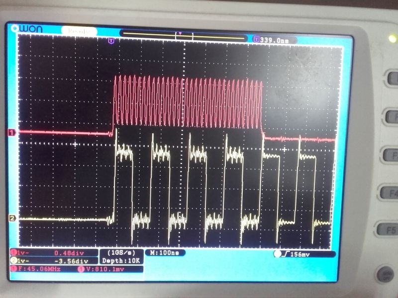
Probably some fine tuning is required to adjust the output delay of the spi_di pin to the spi_ck clock phase. Also, I've replaced the original outc command with outnot for debugging so it always outputs an $AAAA pattern. The result is quite strange. Spi_ck is generated correctly, 32 cycles with sysclk/4=45MHz. However, spi_di is 4 times slower than expected. I thought the rep loop would take 4 clocks per bit but it takes 16.
Could it be that the rep command messes up the instruction fetch FIFO? Fastspin executes from HUBRAM but is normally very fast due to FIFO prefetch. In my case it seems to slow down to 8 clocks per instructions instead of 2. Is this intended or am I doing something wrong? Or just expecting too much?
As my (cheap) flash chips only support 50MHz reads and the P2 is running at 180MHz I have to limit speed to clock/4 anyway so I could do it with bitbanging instead of using the streamer. This is the code I thought should work:
CON	spi_cs = 61
	spi_ck = 60
	spi_di = 59 ' P2 -> flash
	spi_do = 58 ' flash -> P2

	Write_Enable = $06
	Erase_4k     = $20
	Erase_64k    = $D8
	Write_Page   = $02
	Read_Data    = $03
	Read_Status  = $05

PUB Read (hubAdr, flashAdr, size)
' read any number of bytes
  Spi_Init
  Spi_Cmd32 (Read_Data, flashAdr)
  repeat size
    byte[hubAdr++]:= Spi_RdByte
  asm
    drvh	#spi_cs
  endasm

PRI Spi_Init
  asm
		drvh	#spi_cs			'spi_cs high
		fltl	#spi_ck			'reset smart pin spi_ck
		wrpin	#%01_00101_0,#spi_ck	'set spi_ck for transition output, starts out low
		wxpin	#2,#spi_ck		'set timebase to 2 clocks per transition
		drvl	#spi_ck			'enable smart pin
		drvl	#spi_di
  endasm

PRI Spi_Cmd32 (cmd, adr)
' outputs 4 bytes: 8 bit command + 24 bits adr
  asm
		drvh	#spi_cs
		shl	cmd,#24 		'shift command up
		or	cmd,adr			'or in address
		shl	cmd,#1 wc
		drvl	#spi_cs
		wypin	#64,#spi_ck		'start 64 clock transitions
		rep	#2,#32
		outnot	#spi_di
		shl	cmd,#1 wc
.bitout
		drvl	#spi_di
  endasm
Probably some fine tuning is required to adjust the output delay of the spi_di pin to the spi_ck clock phase. Also, I've replaced the original outc command with outnot for debugging so it always outputs an $AAAA pattern. The result is quite strange. Spi_ck is generated correctly, 32 cycles with sysclk/4=45MHz. However, spi_di is 4 times slower than expected. I thought the rep loop would take 4 clocks per bit but it takes 16.
Could it be that the rep command messes up the instruction fetch FIFO? Fastspin executes from HUBRAM but is normally very fast due to FIFO prefetch. In my case it seems to slow down to 8 clocks per instructions instead of 2. Is this intended or am I doing something wrong? Or just expecting too much?
800 x 600 - 97K
Comments
When you read a pin you are actually seeing it as it was a couple of clocks earlier.
When you write to a pin it will not appear until a couple of clocks later.
IIRC I posted a tip in the tricks and traps thread. If not, I think there was a discussion thread about it.
Also, you can find how I do it in the SPI SD code in the rom source. The code runs in hubexec and rcosc which is ~22MHz
As for your code, the rep loop is in hub, so the repeat will need to wait for it’s hub slot to come around again. That’s probably the extra delay your seeing.
Where can I find the source?
Ok, then my expectations were too optimistic. I understand, it's a FIFO not a cache. It has to be reloaded after a jump.
I've unrolled the loop and now it works as expected. This is not perfect but I have to learn how the P2 works. The documentation describes each command and register at the "bare metal" level but I feel like navigating in the fog. It's difficult to guess the idea behind the implementation details and to judge which method out of serveral possibilities is the best for a given situation. And even once you know it's more difficult to find out how it's to be carried out.
Ah, there are "sync serial transmit" and "sync serial receive" smart pin modes. I haven't noticed so far because Chip doesn't use them in his loader code.
sync serial smart pin modes need an external clock at the B input. So they are for SPI slave modes only. For master mode I have to use async serial transmit and receive?
Update:
... no, doesn't work either. the asynchronous modes only work with start and stop bits. Next guess: I have to feed back the clock output pin to the B input with the relative -3..+3 input selector.
The synchronous-serial-transmit smart pin mode looks at a clock input (which is delayed by a few system clocks, and then outputs a data bit which takes a few clocks to get to the pin. So, the output mode has a several-clock turn-around delay from clock input to data output. This limits its speed to maybe Fsysclock/5.
This means if high speed is required synchronous serial receive gives the best performance for reading and streamer output is best for writing because of the limits of the synchronous serial transmit mode. However sysclk/5 is still really fast. I don't think I'll need it.
At the moment, I keep the bitbanging code as it is because it works and optimization is not really needed, here. My parameter file is less than 0.5kB and erasing takes longer than reading or writing, anyway. I found out that it works with 3 or 4 nops.
forums.parallax.com/discussion/169542/p2-links-for-where-to-obtain-tools-sample-test-code-reference-only/p1