

ESD Failure and Fix
 cgracey
Posts: 14,133
cgracey
Posts: 14,133
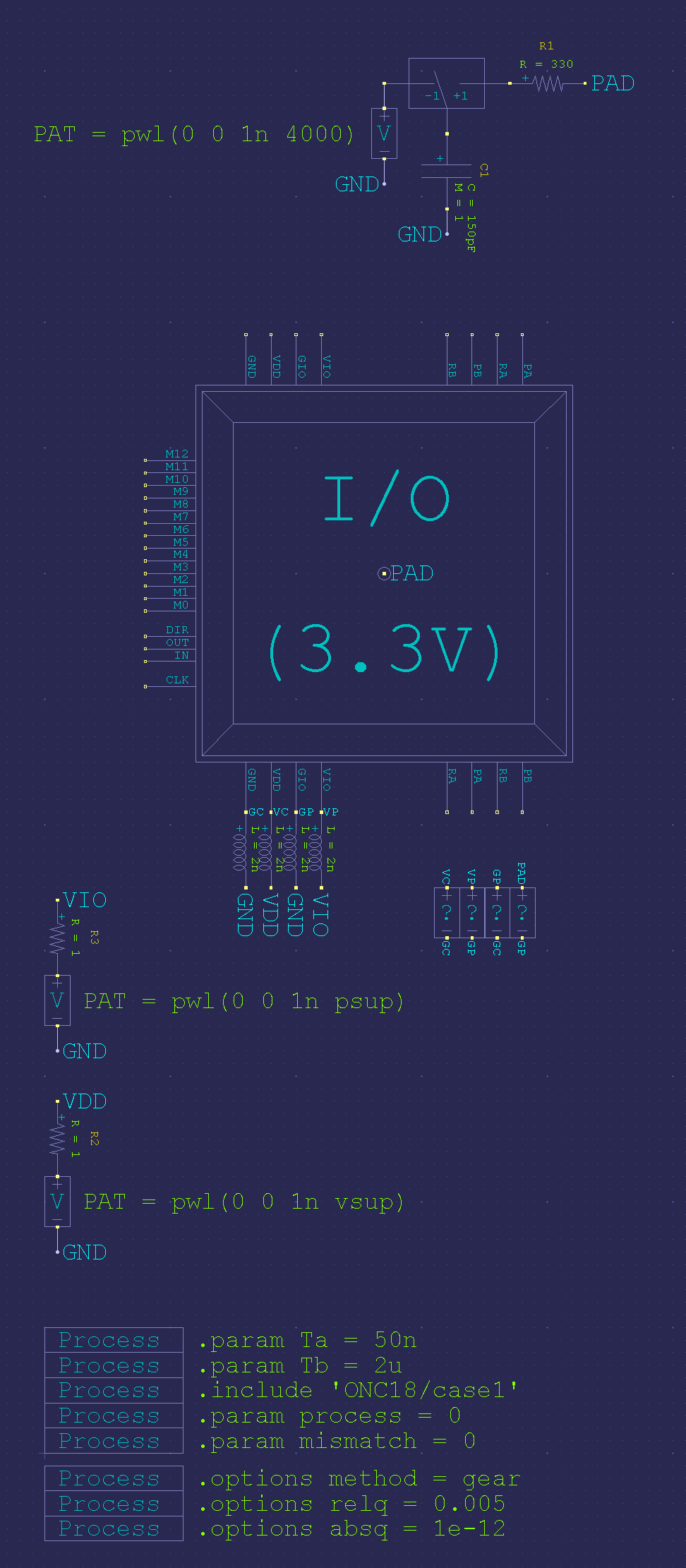
I did some actual ESD zap tests on our previous test chip, which has the same ESD circuits as our current chip that just went off into the shuttle.
The test chip failed miserably, but it was apparent that the 1.8V<-->3.3V logic level translators had been blown out, as other things kept working. I thought that was really peculiar, at first.
It seemed that maybe the GND and GIO signals were getting some big differential voltage between them during zapping. They are not shorted together on the die, but will be both down-bonded to the die paddle on the exposed ground pad of the final package. That's maybe not good enough, though. The test chip is much worse in this regard, as it has longer bond wires and discrete GND and GIO pins (GIO is the 3.3V I/O ground, as opposed to the 1.8V core ground). These long connections have enough inductance to allow plenty of havoc.
To confirm there was a GIO-GND problem, I set up an ESD simulation in SPICE so that I could virtually zap our I/O pad and see what happens. Sure enough, there was a brief 700V disparity between GIO and GND, resulting from the 4kV zap to the pad. Those poor 1.8V NMOS transistors in the level shifters didn't stand a chance.
We need some fast, low-on-resistance clamp between GIO and GND to keep them close together, voltage-wise, during an ESD event. It turns out there's a Schottky diode available in the OnSemi process that seems to be intended just for this sort of application. I know it's for ESD because the default length is 50um, which is huge. I put several of those in parallel in two back-to-back arrangements, one for GIO to GND and another for GND to GIO.
Here are two simulations. On the left is the I/O pad as it's currently designed, and on the right is it with the back-to-back Schottky diodes added between GIO and GND. Also, there's a screenshot of the test setup in SPICE.
We'll get this added into the pad layouts ASAP.

2890 x 2530 - 223K
972 x 2221 - 38K
Comments
I'm a little confused. Unless you have changed the power and ground I/O's significantly, there were already , based on TSMC's guidelines, back to back diodes on ALL of the GIO and GND as well as spark gap structures between all of the Supply's AND grounds. The reason it was built into ALL of the power and ground I/O's was because there was no active circuitry there (i.e. smart pins) leaving tons of space for large ESD and spark gap structures. The spark gap structures were in place with the 2011 test die and proven back then when your ESD zapper still worked. One of my mentors at NSC was a pioneer in ESD structures and techniques to which some of the knowledge I gained was implemented in the 2011 test die design.
Edit: If I remember correctly the breakdown of Air is 30kV per cm ... so that's 3V per micron ... factoring in the dielectric of the ESD structure and the number of distribution fingers in the spark gap we were using, the voltage breakdown was set for around 50V