

Prop2 Analog Test Chip
 cgracey
Posts: 14,133
cgracey
Posts: 14,133
OnSemi is putting us on their May shuttle run for the ONC18 process that the Prop2 is designed in. We were planning on doing this in July, but they got us in earlier.
Tonight I had to divert from the Verilog and make a test chip schematic that Treehouse will lay out in the next week from blocks they've already finished.
The test chip will contain two I/O pins with all the control signals brought to other digital I/O pins. The crystal oscillator pads which contain the RC oscillator, PLL and crystal inverter w/caps is on there, too. The chip also contains the RESET pin, which has a deglitcher and a 20ms one-shot.
We're going to need to use an LQFP-80 package for this, since there is NO logic inside this thing and every internal digital signal is brought to either an INPUT or an OUTPUT pad.
Here's the pinout:
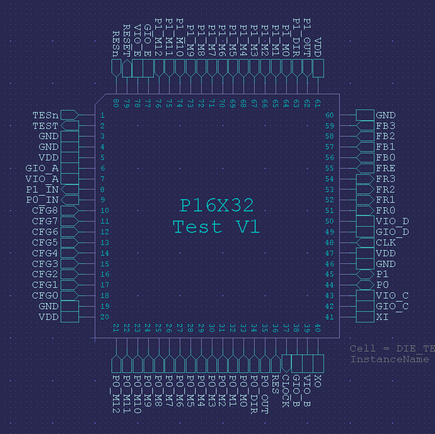
It occurred to me to put ~60k-ohm pull-downs on all the input pins, so that we can use the thing without needing to hook it all up. Also, I didn't want those FB0..FB3 lines to float high and blow the fuses.
We'll make a PCB for this to plug into the -A9 board, so that we can confirm the I/O pins work properly under smart pin control.
I suppose these chips will be back in July.
Tonight I had to divert from the Verilog and make a test chip schematic that Treehouse will lay out in the next week from blocks they've already finished.
The test chip will contain two I/O pins with all the control signals brought to other digital I/O pins. The crystal oscillator pads which contain the RC oscillator, PLL and crystal inverter w/caps is on there, too. The chip also contains the RESET pin, which has a deglitcher and a 20ms one-shot.
We're going to need to use an LQFP-80 package for this, since there is NO logic inside this thing and every internal digital signal is brought to either an INPUT or an OUTPUT pad.
Here's the pinout:
It occurred to me to put ~60k-ohm pull-downs on all the input pins, so that we can use the thing without needing to hook it all up. Also, I didn't want those FB0..FB3 lines to float high and blow the fuses.
We'll make a PCB for this to plug into the -A9 board, so that we can confirm the I/O pins work properly under smart pin control.
I suppose these chips will be back in July.
854 x 852 - 24K
Comments
? Err, why not use the final package here ? (Exposed Pad TQFP 100?) ?
This PAD ring is done, that way you can check the down bonds and any Analog Tests will be on the exact same ground plane & bonding as a final device.
The digital input buffers can be/are disabled in Analog Modes ?
Will this be able to test minimum Iccs of these blocks ? ie unbonded pins default (via reset?) to disabled (and non floating ?)
It's hard to say, until we try it out, but I'm hoping for at least 12 bits. It's delta-sigma, so it may go quite high in resolution. I think it will have very high precision, but probably not as high accuracy.
When it is all on one die frame, the Analog crosstalk noise depends on what else the Logic is doing, and what loads it drives.
This is why some MCUs suggest going into IDLE to get the best ADC results.
eg
10b ADC with on-chip switches, is only 3.3mV of noise on Vcc/Gnd
12b needs better than 805uV
- trying to hit those numbers, on a working MCU, gives an indication of the problem.
If you externally buffer the SDM output, to clean rails, you can do better.
Differential In, referenced to an external low noise reference could help too.
Comes down to what external parts you want to add, to help push down those noise-floors, and what external parts the P2 supports ?
Each four I/O pins have their own 3.3V power and ground connections, just so that the analog can be high quality. The only toggling in the ADC is the differential clock signal, which only goes to the edge of the block.
Yes, there is a May shuttle that we hope to be on.
Are those isolated leads ? I thought the grounds all bused, and bonded to the inner PAD ring ?
If the 3v3 pin are separate, they could be separately filtered for better noise floor.
All this is a good argument for using the same package as the final device for these tests.
Can the Signa-Delta optionally use external parts, to improve performance - eg an external integrator ?
The GIO (ground for I/O) connections bond from the die down to the thermal pad on the final chip. They are not electrically connected to other GIO's and GND on the metal layers. They only meet at the low-Z pad.
The test chip brings out the two I/O pads' GIO and VIO to unique pins, as there is no thermal pad to down-bond to.
The delta-sigma ADC will work best using its own internal circuit, where parasitics are minimized and everything is tightly controlled.
Oh, ok, so the test chip is quite different from the final die, bonding wise.
I was not expecting that.
I guess someone can always use the counters, as SDM-Digital, if they want to externally place Integrator+D.FF, for higher performance ?
Then I guess that the design is custom made (your own design) and you are not using any predesigned "IP block" from OnSemi or Treehouse otherwise you would have complete specs about the number of bits of resolution, INL, DNL, etc...
I remember ADC was one of the five requirements from high volume customers. And I suppose that some of them will ask for at least 12 bits while others may not be happy if the ADC have less than 16 (or 20 bits) don't know. Also some of them will don't care about linearity, INL or DNL, while others would need high linearity to use them for precision measurement. Did you gather that information from them before?
I think is a pitty that we spend so much time on the digital part when maybe the analog part is what makes the propeller different from everything else.
I know it's expensive layout-wise to make capacitive structures on ICs, but it may be worth trying to add some on-die capacitors to the power rails of the analog components. Minimizing the impedance of the buffering on the power rails could mean a few more bits of precision (especially when doing digital processing at the same time). Can under-utilized routing layers be re-purposed to form capacitors?
What size of cap (pF) can you make on the die anyway? I've always assumed since other micros fail to include the crystal caps, that achieving 15-22 pF takes a fair bit of area
Right. Maybe we could get 20pf of bypass in each I/O pad. At 1.5mA, it wouldn't do much. Where caps are needed for the analog sections, there are plenty, per the schematic. There's just no room left for bypass.
You do not get large caps on-die, but anywhere that metal is widened to lower resistance can give a free cap, and Chip has said they have already done a lot of that.
The Caps you get on die, are not really going to improve ADC area noise, but they will 'take the edges off' supply inductance effects, with fast clocking edges, and they also help EMC by giving sorter paths for the highest frequency currents.
Normally, any truly spare space is used as caps, and I'd expect P2 to do the same.
I think some parts do include bulk MLCC caps on the lead frames, and there you can get >> 1nF
20pf bypass is significant at the frequencies where the power/ground pin impedance is large. A quick check with a couple of papers suggests a QFP has a pin impedance on the order of 5nH. If the P2 is running at 100MHz, and you apply the rule of thumb that to make a nice square wave you have harmonics at 100 times the fundamental frequency, the pin impedance is 50 ohms. At these frequencies the 20pF capacitor has an impedance of 5 ohms. If the P2 is running at 200MHz, then the pin is 100ohms and the 20pF cap is 2.5ohms. This may be significant enough to give you some more bits of precision when receiving noise from other parts of the P2.
Can capacitors be made using two interconnect layers, rather than having one of the plates be the bulk silicon?
You can apply cap in several different ways .... layer to layer is most common, but fringe capacitance can actually be greater using interdigitated fingers on the same layer, and then taking that interdigitation a step further by applying the same interdigitation top to bottom on successive layers. Staggering of the top to bottom adjacent layers can increase the effect even further. Fringe capacitance will tend to have slightly greater capacitive effects than a standard parallel plate capacitor because of higher densities at the plate boundary edge.
I know, but stuff I read (admittedly with near-zero expertise) seems to imply that IC capacitors are made using the bulk silicon as one of the plates, for some reason. If you have interconnect layers to solve thorny routing problems in certain places, you might have a lot of interconnect area unused in other places. It seems like the caps would be much cheaper layout-wise if that were the case.