Shop OBEX P1 Docs P2 Docs Learn Events
P2 vs modern process limits — Parallax Forums

P2 vs modern process limits

cgraceycgracey Posts: 14,133
edited 2016-05-02 20:26 in Propeller 2
There are chips under design, already, for 10nm processes that will be 1 inch square (645 mm2). The mask costs, alone, on these will be upwards of $10,000,000.

The P2 is built in a 180nm process and is 0.335 inches on the edge (72 mm2).

A 10nm process is 324x denser than the P2's 180nm process. A 645 mm2 die is 9x bigger than the P2 die. Multiplying those two factors together yields 5,805. That's how much more logic and RAM are on these 1-inch square 10nm chips, compared to the P2.

To put that in perspective, if it were possible to realize that 10nm chip's logic functionality using 180nm process technology, the die would be 76x bigger, on the edge, than the P2. That would make it 25.46 inches on the edge (646mm)!!!

I/we struggle with this relatively simple project, but imagine if we had this much more room to work with:

10nm.png

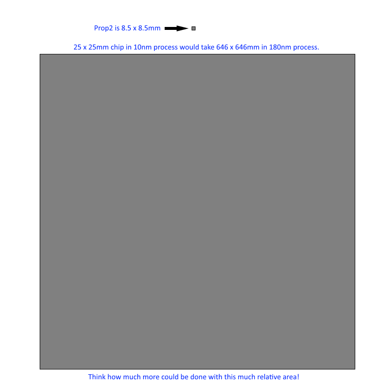
I know... we'd probably die before anything got made.
800 x 800 - 9K
«1345

Comments

  • So, what made you settle on 8.5mm for the P2? Expected yield per wafer? Power considerations? Put another way, why not increase the size to 10mm, for example, to accommodate the full 1MB Hub RAM? Is there a technical issue, or is this more of a marketing/sales concern?
  • jmgjmg Posts: 15,148
    Seairth wrote: »
    So, what made you settle on 8.5mm for the P2? Expected yield per wafer? Power considerations?
    I thought all of that, plus package is a pretty important constraint too.
    E-PAD TQFP100 kind of chooses your die size for you...

  • Maybe a bit more on topic (and somewhat of an explanation of what I was thinking when I posted the prior comment), but I'm always curious what the advantage going to a smaller process would be for something like the propeller, as opposed to just going to a larger die with the existing process.

    Here are the sorts of things I recall others mentioning:

    * Speed. That makes sense, but is there anything that can make the chip faster at 180nm? Less dense circuits (i.e. larger dies for the same design)?

    * Yield. I can somewhat see this, but it seems that the setup cost necessitates an extremely high unit volume to bring the cost in line with the older, cheaper process.

    What else is there, that's only possible at smaller scales?
  • cgraceycgracey Posts: 14,133
    edited 2016-05-02 20:51
    8.5mm was more than enough for the current plan.

    10mm might not have fit the die pad and accommodate the down-bonds for the GND connections.

    The layout is done, now, except for some power metal additions which are coming along.
  • jmg wrote: »
    E-PAD TQFP100 kind of chooses your die size for you...

    Hmm... good point. I would have thought you'd have more room than 8.5mm, but I guess you need a certain amount of room for bonding. Do I remember correctly that the P2 package will be 14mm^2?
  • cgracey wrote: »
    The layout is done, now, except for some power metal additions which are coming along.

    I wasn't suggesting a change. :) If such a change had been reasonable possible, you would have done that one a long time ago, I'm sure. I was just trying to get a better understanding of what the considerations were in choosing the size that you chose.
  • cgraceycgracey Posts: 14,133
    14 x 14mm TQFP-100
  • jmgjmg Posts: 15,148
    cgracey wrote: »
    There are chips under design, already, for 10nm processes that will be 1 inch square (645 mm2). The mask costs, alone, on these will be upwards of $10,000,000.
    ....
    I/we struggle with this relatively simple project, but imagine if we had this much more room to work with:

    Yes, it does show just how much more resource those big players have at their fingertips, but it also shows the risk trade-offs of playing in that space, and teh quite small number of actual design starts.

    Some interesting observations here
    https://www.semiwiki.com/forum/f293/tsmc-7nm-trials-start-next-year-7672.html

    This from Samsung :
    - they cover both leading edge, and 'matured node'
    7nm: we have already begun work on our cost optimized 7LPP node which comes with very competitive PPA scaling.

    8” matured node: keeping in mind there are still ample of new designs and applications that can take advantage of 8in technology, we are opening up our differentiated 8in technologies ranging from 180nm to 65nm, covering eFlash, Power devices, Image sensors and High voltage processes


  • ErNaErNa Posts: 1,742
    This world also works in parallel. So we are on the right track. I know I could do more with P2 than I will do, and that's enough. But the moment you have the leading edge technology available there is one question: is there a low budget market to sell all the computing power in. That could be object recognition, health care, .. music, video, simulation of the sound of wind blowing. ... We will see.
  • jmgjmg Posts: 15,148
    cgracey wrote: »
    8.5mm was more than enough for the current plan.

    10mm might not have fit the die pad and accommodate the down-bonds for the GND connections.

    The layout is done, now, except for some power metal additions which are coming along.

    Have you asked OnSemi about BGA options, and if anything simple needs doing now, to make BGA possible (/ not excluded) as a future package choice ?


  • For those of you who haven't worked it out, Chip's 1" sq in 10nm translates to 92,800 cogs. Projected speed of 160MHz ? , most instructions are 2 clocks in cog execution mode, that works out to 7,424,000 MIPS (combined). My old fashioned calculator only has 6 digits, I had to count on my toes*, too.

    The 1" sq chip in 10nm at 76x quivalent Prop in 180nm on the edge gives an increase from the current 25 pins per edge to 1,900 per edge, or 7,600 EHQFP (exceedingly heavy QFP) package. Presumably there would be a similar increase in mass?

    *No toes were harmed during this act.
  • cgraceycgracey Posts: 14,133
    edited 2016-05-02 22:20
    78rpm wrote: »
    For those of you who haven't worked it out, Chip's 1" sq in 10nm translates to 92,800 cogs. Projected speed of 160MHz ? , most instructions are 2 clocks in cog execution mode, that works out to 7,424,000 MIPS (combined). My old fashioned calculator only has 6 digits, I had to count on my toes*, too.

    The 1" sq chip in 10nm at 76x quivalent Prop in 180nm on the edge gives an increase from the current 25 pins per edge to 1,900 per edge, or 7,600 EHQFP (exceedingly heavy QFP) package. Presumably there would be a similar increase in mass?

    *No toes were harmed during this act.

    Those 92,800 cogs could easily clock at 3, maybe even 4 GHz. You start to realize just how much relative wire time must be involved at those scales.
  • cgraceycgracey Posts: 14,133
    edited 2016-05-02 22:38
    ErNa wrote: »
    This world also works in parallel. So we are on the right track. I know I could do more with P2 than I will do, and that's enough. But the moment you have the leading edge technology available there is one question: is there a low budget market to sell all the computing power in. That could be object recognition, health care, .. music, video, simulation of the sound of wind blowing. ... We will see.

    From jmg's forum link:

    "By the way, sizeable 10nm demand in 2nd quarter 2017 is the iPone 7 refresh of course. " (iPone = iPhone)

    At those nodes, maybe several consumer products drive 80% of demand.

    More from jmg's link:

    "At 14nm, Samsung seems to be doing well here as their fabs in Korea and Texas are running full time, with over 0.5M wafers shipped and defect density below 0.2 defects/cm^2 in production."

    20" wafers???

  • kwinnkwinn Posts: 8,697
    cgracey wrote: »
    ErNa wrote: »
    This world also works in parallel. So we are on the right track. I know I could do more with P2 than I will do, and that's enough. But the moment you have the leading edge technology available there is one question: is there a low budget market to sell all the computing power in. That could be object recognition, health care, .. music, video, simulation of the sound of wind blowing. ... We will see.

    From jmg's forum link:

    "By the way, sizeable 10nm demand in 2nd quarter 2017 is the iPone 7 refresh of course. " (iPone = iPhone)

    At those nodes, maybe several consumer products drive 80% of demand.

    More from jmg's link:

    "At 14nm, Samsung seems to be doing well here as their fabs in Korea and Texas are running full time, with over 0.5M wafers shipped and defect density below 0.2 defects/cm^2 in production."

    20" wafers???

    I think that refers to 500,000 chips shipped.
  • cgraceycgracey Posts: 14,133
    edited 2016-05-02 23:11
    kwinn wrote: »
    cgracey wrote: »
    ErNa wrote: »
    This world also works in parallel. So we are on the right track. I know I could do more with P2 than I will do, and that's enough. But the moment you have the leading edge technology available there is one question: is there a low budget market to sell all the computing power in. That could be object recognition, health care, .. music, video, simulation of the sound of wind blowing. ... We will see.

    From jmg's forum link:

    "By the way, sizeable 10nm demand in 2nd quarter 2017 is the iPone 7 refresh of course. " (iPone = iPhone)

    At those nodes, maybe several consumer products drive 80% of demand.

    More from jmg's link:

    "At 14nm, Samsung seems to be doing well here as their fabs in Korea and Texas are running full time, with over 0.5M wafers shipped and defect density below 0.2 defects/cm^2 in production."

    20" wafers???

    I think that refers to 500,000 chips shipped.

    Oh, duh! Well, wait... wafers, not chips. Over 500,000 wafers were shipped. Probably 300mm wafers.
  • AribaAriba Posts: 2,682
    I've read once that these nm structure sizes under 20nm are just virtual sizes, not real nm sizes. They made some other improvements on the processes and carry this back to a virtual nm size that would repesent the same performance in the older process technology.
    In reality the geometry is bigger, so you can not just scale to a 180nm process to get the yield.
    I read it in a ordinary newspaper, so I'm not sure if it's true.

    Andy
  • jmgjmg Posts: 15,148
    Ariba wrote: »
    I've read once that these nm structure sizes under 20nm are just virtual sizes, not real nm sizes.

    Yes, I think there is an element of 'smoke and mirrors' in some of these 'nm' figures, but I guess as long as everyone agrees on using the same smoke, they still indicate relative improvements ?

    Certainly, you cannot simply scale 10nm:180nm, as very little of the die pushes 10nm, even virtually.
    I've heard these high end devices need very serious clock tree design efforts, with amps involved.
  • Heater.Heater. Posts: 21,230
    78rpm,
    Chip's 1" sq in 10nm translates to 92,800 cogs. Projected speed of 160MHz ? , most instructions are 2 clocks in cog execution mode, that works out to 7,424,000 MIPS
    Puzzle me this...

    If we could build a Propeller with an infinite number of COGs what would it's performance be?

    I suggest zero MIPS.

    Why?

    Because the bandwidth to HUB would be whatever it is now divided by infinity. That is to say zilch.

    There would have to be some serious re-architecting of the Propeller to make any use of 92,800 COGs.

  • jmgjmg Posts: 15,148
    Heater. wrote: »
    Because the bandwidth to HUB would be whatever it is now divided by infinity. That is to say zilch.
    There would have to be some serious re-architecting of the Propeller to make any use of 92,800 COGs.
    Well, yes, but you presume they all access a single, infinite hub too...
    I don't think there is a serious suggestion for 92,800 COGs on the table, just a musing over what the other end of the nm spectrum can give designers to play with.

  • 92,800 cogs! (said while experiencing sharp chest pains)
    If Quartus takes 2 hours to compile Chip's 16 cog verilog code now, even 1000 cogs would take an eternity. :lol:
  • cgraceycgracey Posts: 14,133
    edited 2016-05-03 03:22
    ozpropdev wrote: »
    92,800 cogs! (said while experiencing sharp chest pains)
    If Quartus takes 2 hours to compile Chip's 16 cog verilog code now, even 1000 cogs would take an eternity. :lol:

    I've heard of one-month place-and-route runs. Hopefully, no bug is found three weeks in.

    There is an FPGA cluster made by Cadence called Palladium that costs $1M, I heard. It's for ASIC prototyping. I bet that thing takes a lot of time to compile for. The user's design would have to be partitioned somehow.

    I just now heard our 7-year-old daughter ask her mom, "When you do math REALLY fast, does it knock you out?"
  • evanhevanh Posts: 15,192
    Lol. Surely she's tried and just found it tedious and tiring.
  • Heater.Heater. Posts: 21,230
    jmg,

    Yes, a single infinite HUB. Well we were being absurd, might as well go all the way :)

    More seriously is that it it's Amdahl's law that gets in the way when parallelizing things.

  • cgraceycgracey Posts: 14,133
    edited 2016-05-03 05:54
    evanh wrote: »
    Lol. Surely she's tried and just found it tedious and tiring.

    Yeah, there are limits to the energy you can muster. That's why it can't knock you out. Maybe a yogi could knock himself out, but we are more likely to peter out in a stupor of thought with images of food floating in our minds.
  • ElectrodudeElectrodude Posts: 1,621
    edited 2016-05-03 05:58
    What if you split the hub into multiple hubs, or arranged then in some sort of grid? Imagine a checkerboard, where the black squares are eggbeaters providing 4 rams to the 4 neighboring cogs, and white squares are cogs that have access to the four neighboring hubs?

    Or you could make a tree structure, where groups of 8 or 16 cogs have access to their own local hub, and those hubs are tied into higher-up hubs somehow, which are again tied into higher-up hubs, and so on. This sounds like it would need caches, which sounds disgusting.

    But what would be the point of doing this with the Propeller? If you want to do supercomputing, use a supercomputer.
  • jmgjmg Posts: 15,148
    What if you split the hub into multiple hubs, or arranged then in some sort of grid?

    If HUB access proves too long in P2, another variant would be to split the memory plane, so clusters of 4 can access their shared area in 4 hub cycles and a larger common area could still be 16 Cycles.

    Of course, this adds another memory segment to explain, and for tools to track, and it lowers the peak memory size a Single COG could 'see', but it would cut the latency between closely co-operating COGs.


  • Perhaps a moderator should be advised that someone apparently hacked into Chip's account to create this thread (under Chip's identity). Kidding, of course. But it may be good that Quartus takes so long to compile, such that we get thought-provoking threads like this one.
  • cgraceycgracey Posts: 14,133
    Perhaps a moderator should be advised that someone apparently hacked into Chip's account to create this thread (under Chip's identity). Kidding, of course. But it may be good that Quartus takes so long to compile, such that we get thought-provoking threads like this one.

    I'm almost done adding 1/2/4-bit modes to the streamer. I've got the outputting working. Now, I'm working on the inputting. After this, I'm going to add... it'll be a surprise. It's mainly just a matter of wiring and a mux, but will finish the design.
  • evanhevanh Posts: 15,192
    edited 2016-05-03 08:39
    cgracey wrote: »
    After this, I'm going to add... it'll be a surprise. It's mainly just a matter of wiring and a mux, but will finish the design.

    Yahoo! Guessing time (I'd never do that!) ... Top candidates: Streaming to the LUT, or Streaming to/from Smartpins. Oops, that's way more than some muxing. That leaves Cluso's Cog to Cog latch as a possible.
  • cgraceycgracey Posts: 14,133
    edited 2016-05-03 09:12
    evanh wrote: »
    cgracey wrote: »
    After this, I'm going to add... it'll be a surprise. It's mainly just a matter of wiring and a mux, but will finish the design.

    Yahoo! Guessing time (I'd never do that!) ... Top candidates: Streaming to the LUT, or Streaming to/from Smartpins. Oops, that's way more than some muxing. That leaves Cluso's Cog to Cog latch as a possible.

    I just finished the 1/2/4-bit pin-to-hub streamer input. I still need to test it, though.

    You're on track with Cluso's latch, but it's better than that.
Sign In or Register to comment.