

ATTN: PCBers SUBJECT: New website and exposure box design for your creative needs
 idbruce
Posts: 6,197
idbruce
Posts: 6,197
Hello Everyone
If you like the thought of creating your own circuit boards then you should review this thread entirely. There is a lot of helpful information within this thread pertaining to PCB materials, exposure, developing, photomasks, etc...
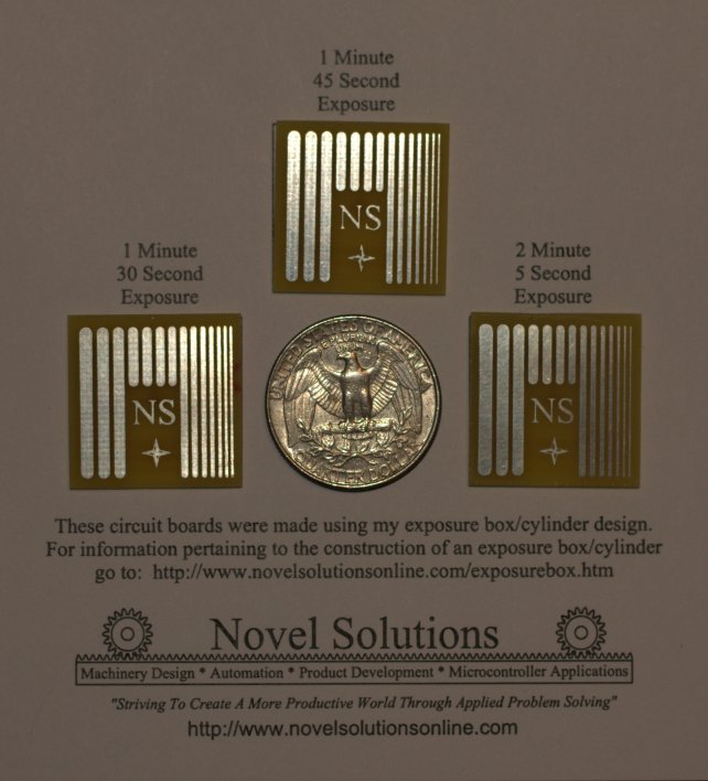
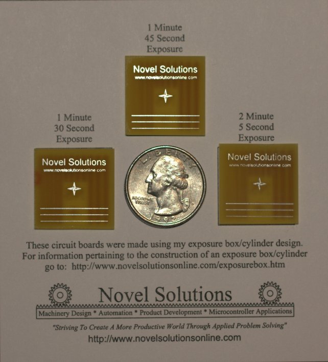
In the photos below you will see a new concept for an exposure box/cylinder and three different samples that it produced. More specific information pertaining the creation of the shown sample can be found in Post #149.
If you like what you see, then visit http://www.novelsolutionsonline.com/exposurebox.htm for detailed construction information. However, please excuse the mess, because the web site is currently under construction.
Bruce
EDIT: Additionally, if you are seriously interested in making PCBs, here is a list of my other threads pertaining to DIY PCBs:
If you like the thought of creating your own circuit boards then you should review this thread entirely. There is a lot of helpful information within this thread pertaining to PCB materials, exposure, developing, photomasks, etc...
In the photos below you will see a new concept for an exposure box/cylinder and three different samples that it produced. More specific information pertaining the creation of the shown sample can be found in Post #149.
If you like what you see, then visit http://www.novelsolutionsonline.com/exposurebox.htm for detailed construction information. However, please excuse the mess, because the web site is currently under construction.
Bruce
EDIT: Additionally, if you are seriously interested in making PCBs, here is a list of my other threads pertaining to DIY PCBs:
ATTN: PCBers SUBJECT: New website and exposure box design for your creative needs
DVD Laser Diode And Optical Block (Future Laser Photoplotter)
DIY PCB Fabrication For The Sake Of Science And Education
Looking For Ideas - Temperature Control
What is the very best way to get a positive image for PCB making these days?
New Project/New Experiment - PCB Etchant And Developer Heaters
http://forums.parallax.com/showthrea...eloper-Heaters
Construction Of A PCB Prototyping Table
http://forums.parallax.com/showthread.php?139308-Construction-Of-A-PCB-Prototyping-Table
Construction Of A Highly Accurate Diamond Blade PCB Cutting Saw
http://forums.parallax.com/showthread.php/156588-Trying-Something-New-Today-My-Latest-Experiment-A-Linear-Slide-Carriage

513 x 507 - 18K
642 x 708 - 63K
642 x 708 - 64K
This discussion has been closed.
Comments
New tool on the way. Please stay tuned
Bruce
I'm probably not the only one with this question.
'
What prints the circut for the PCB layout?....New to this method..sorry???
@Walt - First you make your circuit with a PCB editor, then you print this circuit on a transparency, then you place this transparency over the film on the circuit board and expose it to UV or incandescent light,being dependant on the film. The circuit traces, or absence of circuit traces (positive or negative), again being dependant on the film, allow a photo reaction to the film. This is ultimately what prints the circuit to the board.
Bruce
I checked it out. I have used the Toner Transfer Method a few times it works but not very well. In the near future I would like to do a double sided board. And will reconsider your Exposure Cylinder.
Have a lot on my plate right now and the ELEV8 is coming soon.
For the simple hobbyist like me maybe you could show a sample board in the Cylinder (close up) and then the board etched so we could see the final product. Could be a selling point for you.
Ron
Ron, besides answering questions here, that is my next goal, but I need small sample sizes for doing a lot of testing for better documentation.
With this method, and with my exposure box, cutting accurately sized PCBs to fit the exposure plates can be difficult to say the least. For this equipment, the accuracy of the cut board dimension is detrimental to the alignment of the top copper layer to the bottom copper layer for double sided exposures.
The PCB hobbyist market truly lacks an inexpensive method for cutting PCBs accurately. And it just so happens that I want to create approx. 100 - 1" X 1" sample squares with dimensional tolerances of +.000/-.005. This is both a pain and an opportunity, because as I mentioned earlier, I have a simple idea for a cutter that just might work.
When I am done with my goals, I will have an exposure box, an accurate PCB cutter, and an accurate PCB driller, all for the PCB hobbyist or enthusiast. Additionally, I will be experimenting and documenting the use of inexpensive chemicals for processing the PCBs to make it more appealing to the hobbyist. The samples will be coming soon.
Sounds great, I think your right about there being a market for your products when I was looking for an exposure box a few months ago not much came up on the searches as far as kits there was some complex DIY plans but I like your simple approach. I am interested in your other projects also. Keep up the good work, this hobby is a definitely growing market.
Ron
Thanks for the support. It's funny, this technology has been around for I think a little over a century, and it is hard to find good information on making an exposure box. I was initially going to do the UV led box, but that sounded like to much work.
I made an inaccurate statement and I would like to correct it at this time.
I said:
This is only partially true, although it does make a more professional looking board. However it essential to accurately cut the positive or negatives used for photo imaging to size, especially if small pads are being used to mount devices. Larger pads provide more tolerance in both width and length dimensions, but the top layer image, the bottom layer image, and the PCB material must all be slightly smaller than the perimeter on the exposure plate.
If you want very nice boards with small pads, extreme care must be taken to cut all three within reasonable tolerances. If you use large pads to leave room for error, you can be a little more careless with the tolerances, just as long as all three are slightly smaller than the perimeter of the exposure plate.
Bruce
'
Another qusetion...Are the PC boards coated with the film?...I'm trying to understand how this works.(in the etching stage)
'
Thanks
Yes the boards are either coated with a film or spray.
I did not read this whole article, but it appears to be a very quick down and dirty explanation. I would try to explain it, but many others have already done this for me. I would suggest going to youtube.com and doing a search on "UV + exposure + PCB + etching + developing", always include PCB, but use the rest in various combinations. That way you get to see the whole process in action from start to finish, from UV exposure to etched board.
http://www.ami.ac.uk/courses/topics/0224_img/index.html
If you are tired of soldering a bunch of jumper wires, and just want neater layouts all the way around, this is the way to go.
Bruce
P.S. I watched a slick video the other day, and this guy had it down to a science for using Positiv 20 which is a spray on photo resist, I will get the link off the laptop a little later and post it here, but until then check out youtube. VERY COOL STUFF.
Bruce"
'
Thanks...This does look like the way to go.
Your welcome, and yes it is the way to go, in my opinion. As I go forward with my endeavors, I will have a suite of tools for making this whole process easier and the documentation that will result from all of this should be of benefit to a lot of people. Not all hobbyists will be able to afford my tools, but if they can, it will make the whole process more enjoyable.
At this point in time:
- The exposure box has been designed with plans and parts available at the web site linked above.
- I am currently in the process of making an accurate and automated cutter for PCB boards. Cutting 1/16" boards with a paper cutter can be a bear and there are times when the results are less than desirable, destroying expensive PCB material. Furthermore, this machine will also be able to cut thin sheets of metal.
- The driller is designed, and the blanks for the parts are all cut to size. I just have to drill, thread and assemble.
Just wait until I finish this stuff. There will be ous and ahs.Bruce
Sorry it took so long, but here is a link to the video that I promised the other day. In this video, the author uses Positiv 20 spray on photoresist. I really want to experiment with this stuff, but it is most prevelant in the UK. Wish we had it here in the US and I wish it was readily available.
http://www.youtube.com/watch?v=p2kFazl-aEE
Bruce
'
The link was cool....
'
It be nice for the DIY'ers to have a complete kit to make a finished board.( less the PCB software)
'
By this I mean:
'
1:The rite transparency for the printer
2:The rite board (preconditioned) or the rite spray to use.
3:The rite developer to use.
4:The rite etching solution to use.
5:The needed cleaning chemicals/materials
'
I don't mean that all of this needs to be in the kit, Just what _ALL_the name brand stuff is needed to make a board.I like to have all of my ducks in a row before I start a project like this.
'
Wife keeps asking me what I want for Chistmas....Your UV-Tube is high on the list!
This is also a good article to read pertaining to etching boards. I have not tried this method myself just yet, but there are other people that have and say it works perfectly at a great cost savings.http://www.instructables.com/id/Stop-using-Ferric-Chloride-etchant!--A-better-etc/
And substitute this product for developer to save additional money.http://www.acehardwareoutlet.com/ProductDetails.aspx?SKU=4239216
Now my own personal belief is that applying film photoresist would be nice, if there was a better application system available. I was also thinking about making a tool for applying the film photoresist to smaller size boards. But that will definitely have to wait for a while. I guess I should clarify.... There are actually three options instead of two.
- Spray on photoresist
- Presensitized boards that have photoresist film applied
- You can buy the boards and film seperately and apply the film to the boards.
Each of these options have there pros and cons, so it actually becomes a matter of equipment, experience, cost, and preference. Everybody does it differently, based mostly on the items above.Here is a link to a site that contains some very good information pertaining to PCB processing. If you want more links, I have gobs of them.http://www.thinktink.com/index.htm
Walt, this is the issue.... I want use the spray, but it is not available locally. The presensitzed board are a tad of pain, but it would be perfect, if you could order boards to the exact dimensions that you need them. Like previously mentioned, it can be a bear cutting down the boards, especially if you like 1/16" boards, and keeping the photoresist film in tact during the cutting process.... Well use your imagination.... I believe the solution is to cut bare copper boards to the proper size and then apply the film. Once I get the cutter done, I will do serious experimenting in all directions. But cutting accurately sized boards without destroying my PCB materials is my main objective at this point.
Bruce
I don't have any problems cutting pre-coated board to size, but I don't need much accuracy. It's much easier with CEM-1 material (paper/fibreglass composite) than it is with FR4.
Sometimes I ramble a little bit when trying to express my point, and my point is not always clear, but hey, I try. So I came back to give you another example.
I could not agree more, but as I was trying to point out, everyone has different requirements and needs. To process PCBs on a fairly regular basis, there has to be a system, and the process should be at least somewhat organized. To make it all worthwhile and cost effective, a person must feel the way you stated it: .
The materials and equipment for processing your own PCBs can be quite costly. So reducing this cost is of the utmost importance, especially to some people. To illustrate my point more effectively, let me give you an example. The photoresist is exposed by light. So of course it is only natural to use the most translucent material possible for your positive or negative. Transparent films for the printer are also quite costly, but some people use tracing paper or vellum to reduce this cost. Tracing paper and vellum is not nearly as translucent as transparent films, so naturally it takes longer to expose the photoresist. PCB processors must weigh certain values, such as time versus cost. Drilling PCBs can also be used as an example. Can FR4 be drilled with a standard drill bit? Yes it can, but the drill bit will dull rather rapidly, that is why carbide drills or carbide tipped drills are the industry standard. A person must weigh how often they will produce PCBs, the cost of material, the cost of equipment, time, etc.... My best advice is to read, read, and read to determine the process that will fit nicely into your budget and time allotment. I can provide advice and suggest materials, but only you can decide how much you can afford and how fast you want the process to be.
Give me a day or so and I will provide you with the links to some very good reading material so that you can determine the method and process to best suit your needs and budget.
Bruce
@Walt - Here is another quick link to an informative site http://www.frezycnc.eu/pcb-processing-manual/
EDIT: If and when I decide to make a film laminator, I will then sell film coated boards to match the size of my standard exposure plates and custom made exposure plates.
Please explain.
Here is something I found on applying the film using wet lamination:
http://members.optusnet.com.au/eseychell/PCB/photoresist/Wet_Lamination_of_Photoresist_for_Hobbyists.pdf
That was a nice article.